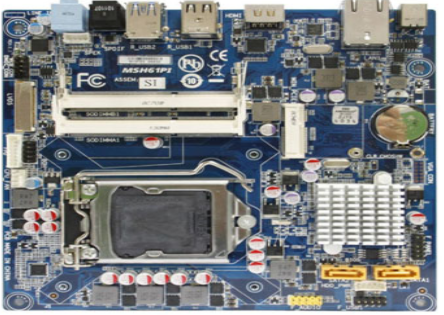
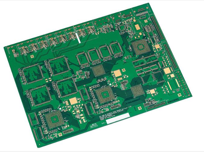
PCB EMI design specification steps
1. IC power processing
1.1) Ensure that each IC power PIN has a 0.1UF decoupling capacitor. For BGA CHIP, there are 8 capacitors of 0.1UF and 0.01UF in the four corners of the BGA. Pay special attention to the addition of filter capacitors, such as VTT, for the power supply of the trace. This not only has an impact on stability, but also has a great impact on EMI.
2 Handling of the clock line
2.1) It is recommended to run the clock line first.
2.2) For clock lines with a frequency greater than or equal to 66M, the number of vias per line shall not exceed 2, and the average shall not exceed 1.5.
2.3) For clock lines with a frequency less than 66M, the number of vias per line shall not exceed 3, and the average shall not exceed 2.5
2.4) For clock lines longer than 12 inches, if the frequency is greater than 20M, the number of vias should not exceed 2.

2.5) If the clock line has a via hole, add a bypass capacitor between the second layer (ground layer) and the third layer (power layer) at the adjacent position of the via hole to ensure that the reference layer is changed after the clock line is changed. The loop of the high frequency current (adjacent layer) is continuous. The power layer where the bypass capacitor is located must be the power layer through which the via passes, and be as close as possible to the via. The maximum distance between the bypass capacitor and the via should not exceed 300MIL.
2.6) In principle, all clock lines cannot pass through islands. Here are four scenarios for crossing the island.
2.6.1) The cross-island appears between the power island and the power island. At this time, the clock line is routed on the back of the fourth layer, the third layer (power layer) has two power islands, and the fourth layer must cross these two islands.
2.6.2) Cross-island appears between the power island and the ground island. At this time, the clock line is routed on the back of the fourth layer, and there is a ground island in the middle of a power island on the third layer (power layer), and the fourth layer must cross these two islands.
2.6.3) Cross-island appears between the earth island and the strata. At this time, the clock line is routed on the first layer, and there is a ground island in the middle of the second layer (ground layer), and the wiring of the first layer must cross the ground island, which is equivalent to the ground line being interrupted.
2.6.4) There is no copper under the clock line. If the conditions are limited, it is impossible to not cross the island, ensure that the clock line with a frequency greater than or equal to 66M does not cross the island. If the clock line with a frequency less than 66M crosses the island, a decoupling capacitor must be added to form a mirror path. Place a 0.1UF capacitor between the two power islands and close to the clock line across the island.
2.7) When faced with the choice of two vias and one through the island, choose one through the island.
2.8) The clock line should be more than 500MIL away from the edge of the I/O side board, and do not run alongside the I/O line. If it is not possible, the distance between the clock line and the I/O port line should be greater than 50MIL.
2.9) When the clock line is on the fourth layer, the reference layer (power plane) of the clock line should try to supply power to the power plane of the clock. The less clocks referenced to other power planes, the better. In addition, the frequency is greater than or equal to 66M The reference power plane of the clock line must be a 3.3V power plane.
2.10) The line spacing of the clock line should be greater than 25MIL.
2.11) The incoming line and outgoing line should be as far as possible when the clock line is connected.
2.12) When the clock line is connected to BGA and other devices, if the clock line changes layers, try to avoid vias under the BGA.
2.13) Pay attention to each clock signal, don't ignore any clock, including AC_BITCLK of AUDIO CODEC, especially FS3-FS0. Although it is not a clock from the name, it is actually a clock, so be careful.
2.14) The clock chip pull-up and pull-down resistors should be as close as possible to the clock chip.
3. I/O port processing
3.1) Each I/O port including PS/2, USB, LPT, COM, SPEAK OUT, GAME is divided into one ground, the leftmost and rightmost are connected to the digital ground, and the width is not less than 200MIL or three vias. Do not connect with other places. Digitally connected.
3.2) If the COM2 port is pin-type, it should be as close as possible to the I/O ground.
3.3) I/O circuit EMI device is as close as possible to I/O SHIELD.
3.4) The power layer and the ground layer at the I/O port are separately islanded, and the Bottom and TOP layers should be laid on the ground, and the signal is not allowed to pass through the island (the signal line is directly pulled out of the PORT, and the I/O PORT is not routed for a long distance) .
4. A few notes
A. The design engineer must strictly abide by the PCB EMI design specification. The EMI engineer has the right to inspect. If the PCB EMI design specification is violated and the EMI test FAIL is caused, the responsibility shall be borne by the design engineer.
B. The EMI engineer is responsible for the design specifications and strictly abides by the PCB EMI design specifications, but still EMI tests FAIL. The EMI engineer is responsible for providing solutions and summarizing them in the PCB EMI design specifications.
C. The EMI engineer is responsible for the EMI test of each peripheral port, and the test shall not be missed.
D. Each design engineer has the right to suggest and question the design specification. EMI engineers are responsible for answering questions and adding design specifications to the engineers’ suggestions after being verified through experiments.
E. EMI engineers are responsible for reducing the cost of PCB EMI design and reducing the number of magnetic beads used.