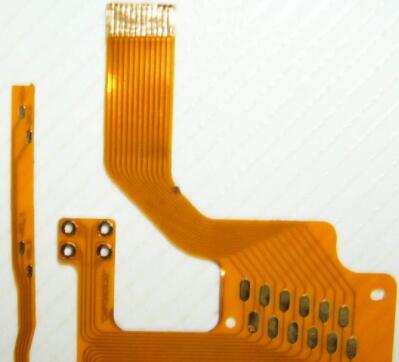
Flexible circuit board is a highly reliable and excellent flexible printed circuit board made of polyimide or polyester film as the base material. Referred to as soft board or FPC.
Features: It has the characteristics of high wiring density, light weight, and thin thickness; it is mainly used in many products such as mobile phones, notebook computers, PDAs, digital cameras, LCMs, etc.
FPC types include
has a chemically etched conductive pattern, and the conductive pattern layer on the surface of the flexible insulating substrate is a rolled copper foil. The insulating substrate can be polyimide, polyethylene terephthalate, aramid cellulose ester and polyvinyl chloride. Single-layer FPC can be divided into the following four sub-categories:
1. The single-sided connection wire pattern without covering layer is on the insulating substrate, and the wire surface has no covering layer. The interconnection is realized by soldering, welding or pressure welding, which is commonly used in early telephones. 2. Compared with the previous type, the single-sided connection with a covering layer only has an extra layer of covering layer on the surface of the wire. The pads need to be exposed when covering, and it can simply be left uncovered in the end area. It is the most widely used and widely used single-sided flexible PCB. It is used in automotive instruments and electronic instruments.
3, double-sided connection without covering layer
The connection pad interface can be connected on the front and back of the wire. A via hole is opened on the insulating substrate at the pad. This via hole can be punched, etched or made by other mechanical methods at the required position of the insulating substrate. become.

4, double-sided connection with covering layer
The front type is different, the surface has a covering layer, and the covering layer has via holes, allowing both sides to be terminated, while still maintaining the covering layer. It is made of two layers of insulating materials and a layer of metal conductors. Circuit board PCB
2, double-sided FPC
Double-sided FPC has a conductive pattern made by etching on both sides of the insulating base film, which increases the wiring density per unit area. The metallized hole connects the patterns on both sides of the insulating material to form a conductive path to meet the design and use function of flexibility. The cover film can protect single and double-sided wires and indicate where the components are placed. According to requirements, metallized holes and cover layers are optional, and this type of FPC has fewer applications.
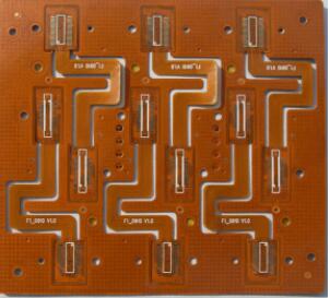
3, multilayer FPC
Multi-layer FPC is to laminate 3 or more layers of single-sided or double-sided flexible circuits together, and form metallized holes by drilling and electroplating to form conductive paths between different layers. In this way, there is no need to use a complicated welding process. Multilayer circuits have huge functional differences in terms of higher reliability, better thermal conductivity and more convenient assembly performance.
FPC manufacturing process
Almost all the FPC manufacturing processes so far have been processed by the subtractive method (etching method). Usually, a copper clad board is used as a starting material, a resist layer is formed by photolithography, and the unnecessary part of the copper surface is etched and removed to form a circuit conductor. Due to problems such as undercutting, the etching method has limitations in the processing of fine circuits.
Because it is difficult to process or maintain high-yield micro circuits based on the subtractive method, the semi-additive method is considered to be an effective method, and various semi-additive methods have been proposed. An example of micro-circuit processing using the semi-additive method. The semi-additive process starts with a polyimide film, and first casts (coats) a liquid polyimide resin on a suitable carrier to form a polyimide film.
Next, a sputtering method is used to form a seeding layer on the polyimide base film, and then a resist pattern of the reverse pattern of the circuit is formed on the seeding layer by photolithography, which is called a plating resistant layer. The blank part is electroplated to form a conductor circuit. Then remove the resist layer and unnecessary seeding layer to form the first layer of circuit. Coating photosensitive polyimide resin on the first layer of circuit, using photolithography to form holes, protective layer or insulating layer for the second layer of circuit layer, and then sputtering on it to form a seeding layer, as the second The base conductive layer of a two-layer circuit. By repeating the above process, a multilayer circuit can be formed.