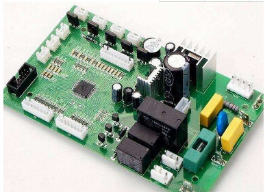
The following mainly introduces the documents needed for the PCB board to be sent to the SMT chip processing factory
One, the required documents
1. BOM list Component list
2. No welding list
3. SMT coordinate file
4. Schematic diagram of the device
5. List of manual soldering components
6. Make PCB for stencil file
2. Description of the production steps and methods of each document
1. BOM list Component list
2. No welding list
3. SMT coordinate file
4. Product silk screen image (recommended to be made in DXP)
(1) Schematic diagram of top surface parameters
(2) Schematic diagram of the number on the top surface
(3) Schematic diagram of bottom surface parameters
(4), schematic diagram of bottom surface parameters
5. List of manual soldering components
6, PCB board steel mesh file
3. Detailed description of the production steps and methods of each document

1. BOM list Component list
Production method: export it in the schematic diagram and then organize it
Export method: The method in protel and DXP is the same, it is recommended to export in DXP
Select [Reports/Bill of Material] on the interface, and then directly select Next until Finish
2. No welding list
Organize according to the first step component list
3. Methods and steps for exporting SMT coordinate files:
(1) Select [File / Open…] to open a .PCB file;
(2), click TopLayer, select [Edit / Select / All on Layer] all on the layer;
(3), click BottomLayer, select [Edit / Select / All on Layer] all on the layer;
(4) After finishing, press Shift + Delete to delete the redundant lines on the Top and Bottom sides;
(5) Select [Design / Options…], turn on the Layers button, select [Toplayer]/[BottomLayer] under Singal Layers, then select [Top Overlay]/[BottomLayer] under Silkscreen, and then select Other under Of [Keepout];
Note: You can also turn off Top and Bottom separately to make it clearer.
(6) After completing the above steps, the position of the pad silk screen can be clearly displayed;
(7) Select [Edit / Origin / Set] to set the origin position (* After setting the PCB origin position, remember that the PCB origin position on the machine should also be set here);
(8) Select [File/CAM Manager..] in the export wizard, select Pick Place, check Text, keep clicking Next, select Metric as the unit, and finish generating a Pick Place file, select and press F9 Generate CAM files;
(9). Find the Pick Place.. file in the CAM for.. directory of the [Explorer] window on the left, right-click and export to the target path you want;
(10) Then open the Pick Place file with Excel and organize it into the files required by SMT, where Mid X and Mid Y are the X and Y coordinates required by SMT.
Note: TopLayer and BottomLayer should be separated when sorting
4. The pdf file of the screen printing diagram of the product component position (recommended to be made in DXP)
(1) Schematic diagram of top surface parameters
The schematic diagram of the top surface parameters is the resistance and capacitance of the TopOverlay layer, the resistance value of the IC, the capacitance value, the name of the IC, etc. (10K, 1UF, MAX354, etc.)
Note: All parameters are best to be centered (within the silk screen of the pad)
Steps and methods:
A, Open a PCB file in DXP
B. Choose to display only TopOverlay and KeepOutLayer
C. Hide the device number, only display the device parameters, put the parameters of each device within the silk screen of the pad, put it in the middle, pay attention to the consistency of order and direction
D, select [File/Smart PDF…] to export to PDF file
Note: Figures 2, 3, and 4 indicate that only TopOverlay and KeepOutLayer layers are selected to be output
Left mouse button to select layer, right mouse button to select delete layer and add layer
Delete is to delete a layer; Insert Layer is to add a layer
(2) Schematic diagram of the number on the top surface
The schematic diagram of the top surface number is the number of the resistance, capacitance, and IC of the TopOverlay layer (R1, C1, U1, etc.)
Note: All numbers are best to be centered (within the silk screen of the pad)
Steps and methods:
A, Open a PCB file in DXP
B. Choose to display only TopOverlay and KeepOutLayer
C. Hide the device parameters, only display the device number, put the number of each device within the silk screen of the pad, put it in the middle, pay attention to the consistency of order and direction
D, select [File/Smart PDF…] to export to PDF file
The details are the same as the first step above
(3) Schematic diagram of bottom surface parameters
The schematic diagram of the bottom surface parameters is the resistance, capacitance, IC resistance, capacitance, IC name, etc. of the BottomOverlay layer (10K, 1UF, MAX354, etc.)
Note: All parameters are best to be centered (within the silk screen of the pad)
Steps and methods:
A, Open a PCB file in DXP
B. Choose to display only BottomOverlay and KeepOutLayer
C. Hide the device number, only display the device parameters, put the parameters of each device within the silk screen of the pad, put it in the middle, pay attention to the consistency of order and direction
D, select [File/Smart PDF…] to export to PDF file
The detailed steps are basically the same as the first step above
(4), schematic diagram of bottom surface parameters
The schematic diagram of the number on the bottom surface is the number of the resistors, capacitors, and ICs of the BottomOverlay layer (R1, C1, U1, etc.)
Note: All numbers are best to be centered (within the silk screen of the pad)
Steps and methods:
A, Open a PCB file in DXP
B. Choose to display only BottomOverlay and KeepOutLayer
C. Hide the device parameters, only display the device number, put the number of each device within the silk screen of the pad, put it in the middle, pay attention to the consistency of order and direction
D, select [File/Smart PDF…] to export to PDF file
The details are the same as the third step above
5. List of manual soldering components
Organize according to the BOM list
6, PCB board steel mesh file
This file is provided by the hardware department