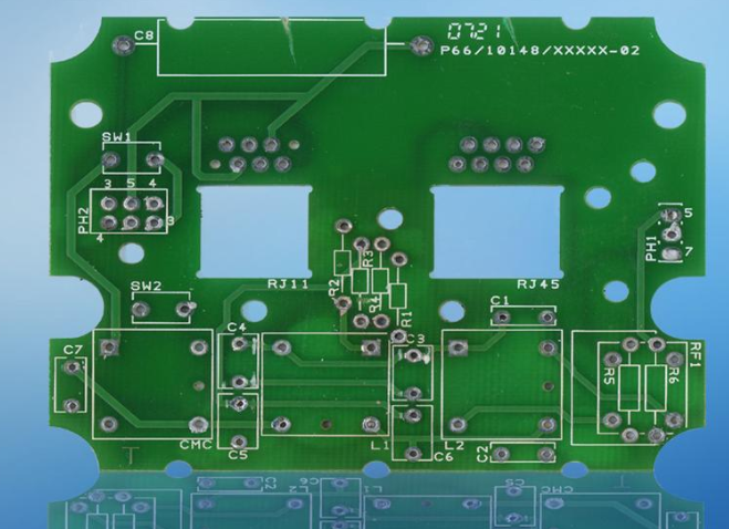
The role of the PCB. The function of the PCB is to provide a base for completing the first-level assembly of components and other necessary electronic circuit board parts to form a module or finished product with a specific function. Therefore, in the entire electronic product, the PCB plays the role of integrating and connecting all the functions of the assembly. Therefore, when the electronic product malfunctions, the first question is often the PCB.
The evolution of PCB 1. As early as 1903, Mr. Albert Hanson pioneered the use of the concept of "Circuit" to be applied to the telephone exchange system. It is cut into circuit conductors with metal foil and glued to paraffin paper, which is also pasted with a layer of paraffin paper, which has become the prototype of the current PCB mechanism. By 1936, Dr Paul Eisner truly invented the PCB manufacturing technology and issued a number of patents. Today's print-etch (photo image transfer) technology is inherited from its invention.
PCB types and manufacturing methods are diversified in materials, levels, and production processes to suit different electronic products and their special needs.

PCB double panel
Cutting, drilling, copper plating, plate surface plating, pattern transfer, pattern plating, etching, quality inspection, printing solder mask (green oil/white characters), immersion gold, tin spray, gold plating, V-CUT gong, beer house test FQC packaging finished product warehouse shipment
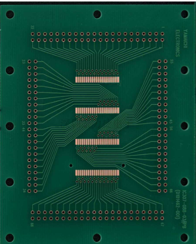
PCB multilayer board
Cutting Inner layer DF AOI Browning Press plate Drilling room Immersion copper Plate plating Outer layer DF Outer layer etching QC11 Green oil, white letters Immersion gold, spray tin, gold plating V-CUT Gong room, beer room Test FQC packaging Finished product warehouse Shipment
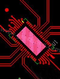
PCB copper surface treatment (brushing)
Printing ink (screen printing ink has different meshes, generally 77T or 57T)
Pre-baked (different ink parameters are different, generally 75-80 degrees)
Exposure (exposure energy level 10-12)
Development (55% development point)
Visual inspection-
Post curing (150 degrees 60 minutes)
The PCB production process is divided into several aspects, divided into single-panel process, double-panel process, and the other is the multi-layer board process. In addition to the general hard board, the soft board is also a flexible boardFPC. There are also several processes., That is, single-layer FPC, multi-layer FPC, etc.
Sometimes we think that the production process of printed circuit boards is a very complicated matter. Here is an analysis of the production process of vaguely printed circuit boards. First of all, we need to know the function and role of the printed circuit board. The first step is to provide a base for the completion of the first level of assembly and other necessary electronic circuit parts to form a module or finished product with a specific function. Therefore, the printed circuit board process is in the entire electronic product, almost all kinds of electronic equipment, from electronic watches, to computers, to communication electronic equipment, and finally to military weapon systems. As long as there are electronic components such as integrated circuits, For the electrical interconnection between them, it will be used.
The production process of printed circuit boards is generally divided into three types: single-sided, double-sided and multi-layer boards. Different factories with different production processes are called differently, but the principle of the process flow is the same!
The single-panel production process is easier to understand than the double-panel process. Basically, it is cutting-drilling-graphics transfer-etching-solder mask and printing-metal surface treatment-finished product molding-testing and inspection-packaging Shipment.
The overall process of double panel production is: cutting-drilling-electroless copper plating and copper plating-pattern transfer-pattern plating and protective tin plating-etching-intermediate inspection-solder mask- Printed characters-metal surface treatment-finished product molding-electrical testing-appearance inspection-packaging and shipment.
The multi-layer PCB board process is to increase the inner layer process before the double-sided process. The basic process: cutting-inner layer graphics transfer-inner layer etching-inner layer etching inspection-copper surface oxidation treatment-typesetting and lamination Board-pressing board-cutting board forming-followed by double-sided board process.
The above is the production process of printed circuit boards. The printed circuit boards have developed from single-layer to double-sided and multi-layer boards, and have maintained their respective development trends. Because it has been continuously developing in the direction of high precision and high density, continuously reducing the volume, reducing the cost, and better using the printed circuit board in the future development of electronic equipment, it will continue to have strong vitality.