Definition of pcb lamination:
It is the process of bonding each layer of a circuit board into a whole. The entire process includes kiss pressure, total pressure, and cold pressure. During the kiss pressing stage, the resin penetrates into the bonding surface, fills the gaps in the pipeline, and then enters full pressure bonding to all gaps. The so-called cold pressing refers to the rapid cooling of circuit boards to maintain dimensional stability.
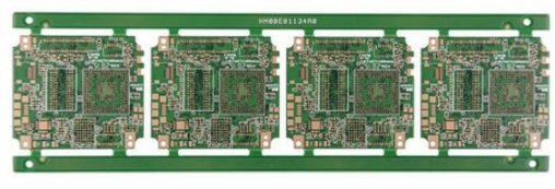
In circuit board manufacturing, lamination is carried out after applying the inner layer to the PCB. Made of substrates, laminates, solder mask, and screen printing.
The steps of the pcb lamination process flow:
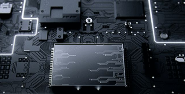
The pcb lamination process is a process of combining multiple layers of materials together to form a single structure. Typically, circuit boards are made of thin copper layers located internally between thermosetting resin substrates. This process stacks multiple single-layer PCB boards together and then presses them into an ordered, multi-layer structure, including an electrical connectivity mode.

1. The first step is to prepare the PCB board. Each single-layer board must undergo chemical drilling and contour processing before being combined into a multi-layer structure. At this stage, cutting, splicing, and thickness measurement are required.
2. The second step is copper plating treatment. In this step, the prepared PCB board needs to be copper plated to enhance its conductivity.
3. The third step , board layer sequence. Before combining single-layer boards into multi-layer boards, they must be stacked together in the correct order. CAD software is usually used to design the correct layer sequence.
4. The four step, ink printing. This step uses targeted ink to print necessary markings and patterns. These markings and patterns are helpful for the subsequent assembly and manufacturing of the board layers.
5. Step 5, press. Once all single-layer boards are assembled and printed, they can be combined into a multi-layer structure through a pressing process. Usually, a thermal compressor is used for curing.
6. Step 6, electrical connection. Connecting multiple layers of PCB boards to each other and connecting external components is the final step. Connect the components of each layer through drilling holes and connect external and internal components to complete the electrical connection of the PCB board.
The importance of pcb lamination process flow:
The pcb lamination is an important component of the electronic manufacturing industry. The importance of this process lies in:
1:Improving production efficiency
The pcb lamination process can manufacture multiple PCB boards simultaneously, thus improving production efficiency. This helps to meet the demand for going to the market and improve customer satisfaction.
2:Improving Quality
The pcb lamination process can ensure the integrity and reliability of the PCB board. This can maintain the consistency of PCB boards in the ecosystem and improve their quality standards.
3:Improving PCB Design
The pcb lamination process provides designers with new design possibilities, which can control the thickness, number of layers, and arrangement of the board, and improve the integration level of the device without damaging signal transmission.
The pcb lamination process is one of the most important processes in PCB board manufacturing. It involves the assembly, printing, and hot pressing processes of the board. Properly executing these processes will help improve production efficiency, meet market demand, and improve the quality and design of PCB board.