When it comes to PCB, novices often confuse PCB schematic and PCB design documents, but in fact they refer to different things. Understanding the differences between them is the key to successful PCB manufacturing. Therefore, in order for beginners to better complete this, this paper will decompose the key differences between PCB schematic and PCB design.
Before understanding the difference between schematic diagram and design, what you need to know is, what is PCB?
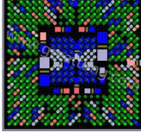
One of the key components in electronic products is the printed circuit board (PCB). This is a very basic component. PCB looks like layers of different materials pressed together by heat and adhesive.
What is PCB schematic diagram?
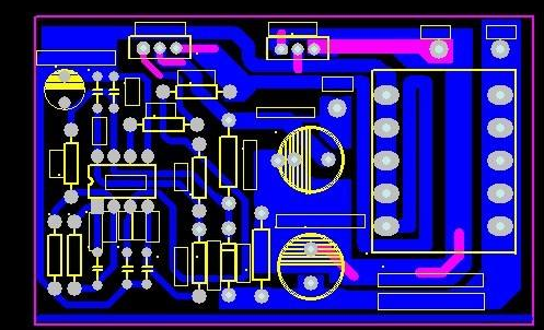
PCB schematic diagram is a simple two-dimensional circuit design, showing the functions and connections between different components
Therefore, PCB schematic diagram is the first part of PCB design. This is a graphical representation that uses agreed symbols to describe circuit connections, whether in written or data form. It also prompts the components to be used and how they are connected.
PCB schematic diagram is a plan and blueprint. It does not indicate the specific location of the component. On the contrary, the schematic diagram outlines how the PCB will finally realize the connection and forms a key part of the planning process.
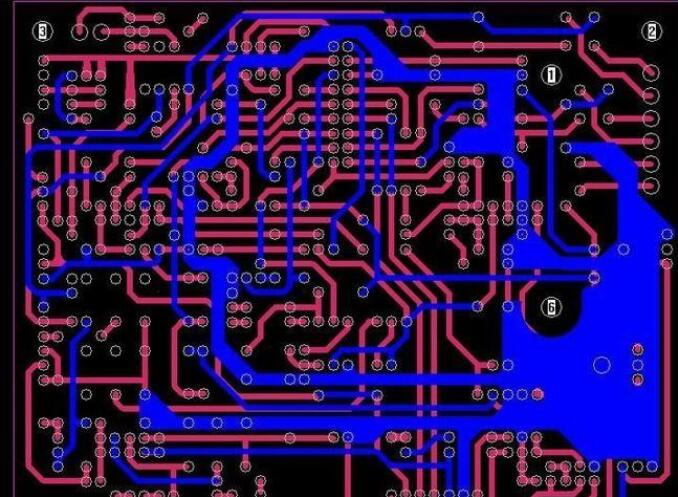
The schematic diagram is a diagram showing the principle of connection between components on the circuit board. In the forward research such as scheme development, the function of schematic diagram is very important, and the control of schematic diagram is also related to the quality of the whole project. Extending from schematic diagram will involve PCB layout, that is, PCB wiring. Of course, this kind of wiring is based on the schematic diagram. Through the analysis of the schematic diagram and the restriction of other conditions of the circuit board, the designer can determine the location of components and the number of layers of the circuit board. It represents only the virtual connection relationship, which is used to guide PCB designers to connect according to the connection relationship of schematic diagram.

What is PCB design?
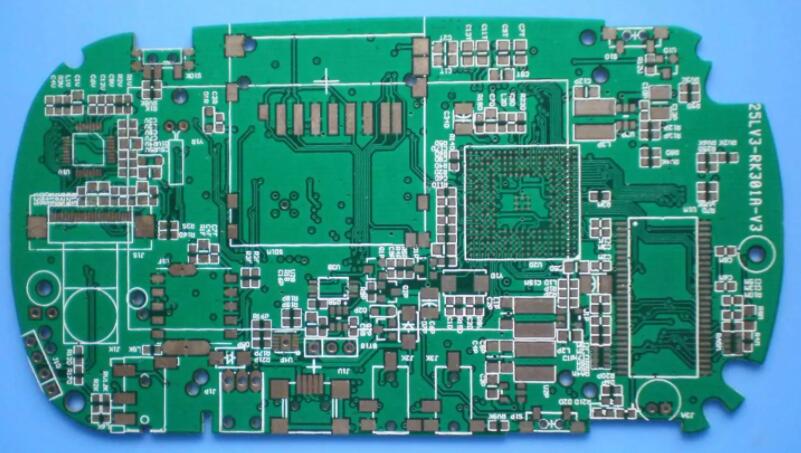
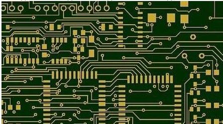
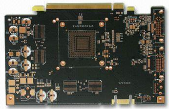
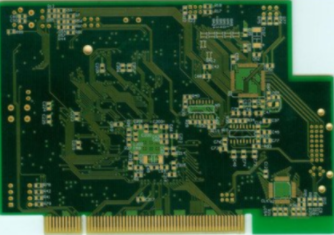
The PCB is designed as a three-dimensional layout, marking the position of components after ensuring the normal operation of the circuit.
PCB design is a performance-related stage. Engineers build real components based on PCB design so that they can test whether the equipment works normally. As we mentioned earlier, anyone should be able to understand PCB schematic diagram, but it is not easy to understand its function by viewing the prototype.
After completing these two stages, if you are satisfied with the performance of the PCB, you need to implement it through the manufacturer.
Composition of PCB schematic diagram
After roughly understanding the difference between the two, let's take a closer look at the elements of the PCB schematic. As we mentioned, all connections are visible
In order to clearly see the connections between electronic components, they are not created in proportion. In PCB design, they may be very close to each other, and some connections may cross each other, which is actually impossible. Some links may be located on the other side of the layout, with marks indicating that they have been linked. This PCB blueprint can use one page, two pages or even several pages to describe all the contents that need to be included in the design. Finally, note that, More complex diagrams can be grouped by function to improve readability. The connection arrangement in this way will not occur in the next stage, and the schematic diagram usually does not match the final design of the 3D model.
About PCB design
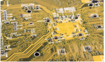
At this stage, we transition from PCB schematic diagram to physical representation constructed with laminated materials or ceramic materials. When a particularly compact space is required, some more complex applications need to use multilayer PCBs.
The content of the PCB design file follows the blueprint established by the schematic flow, but as mentioned earlier, the two are very different in appearance. But what differences can be observed in the design documents?
When we talk about PCB design files, we are talking about 3D models, including PCB and design files. They can be single or multiple layers, but the most common is two layers.
We can observe some differences between PCB schematic and PCB design documents
1. The size and position of all components are correct
2. If two points should not be connected, they must bypass or switch to another PCB layer to avoid crossing each other on the same layer
In addition, as we briefly discussed, PCB design pays more attention to actual performance, because this is to some extent the verification stage of the final product. At this time, the practicality of the design must play a role, and the physical requirements of the PCB must be considered.
These include
1. How to allow sufficient heat distribution between parts
2. Connector at the edge
3. About current and heat, how thick must all traces be
4. Because physical limitations and requirements mean that PCB design documents are usually very different from the designs on schematic diagrams, the design documents include a screen layer. The screen layer indicates letters, numbers and symbols to help engineers assemble and use PCBs.
5. After all components are assembled on the PCB, it is required to work as planned. If not, you need to redraw.
Although PCB schematic and PCB design files are often confused, in fact, when creating a PCB, making PCB schematic and PCB design refer to two independent processes. PCB schematic diagram capable of drawing process flow must be created before PCB design, which is an important part of determining PCB performance and integrity.