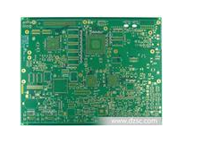
The difference between the full length of the circuit board and the film
Long board/ultra-long board circuit board film: usually the processing technology people talk about, and the applied potion is acid-alkali etching process film is due to the route or route required after the film photo is made. The copper surface is fully transparent, and the unacceptable part is gray-black. After being exposed through the route processing process, the fully transparent part is oxidized and hardened due to the wet film resist being irradiated by the sun, and the next developer solution The processing technology will wash away the wet film without hard bottoming. Therefore, the ultra-long board circuit board only bites the wet film and washes away a part of the copper (the gray-black part of the film photo) during the etching process, and saves the wet film. Not washed away belongs to the route we want (a part of the film photo that is completely transparent)
The whole piece of the ultra-long board circuit board: usually the patTri processing technology that people talk about, and the potion used is the alkaline etching process. Part of it is fully transparent. After being exposed through the same route processing process, the fully transparent part is hardened due to the oxidation of the wet film resist by the sun. The next developer processing technology will make it harder The wet film is washed away, followed by the tin-lead electroplating process. The tin-lead is plated on the copper surface washed away by the wet film in the previous processing process (developing solution), and then the film is removed (removing the hard bottom due to sunlight) Wet film), and in the next etching process, use alkaline xian water to cut off the copper pool that is not maintained by tin and lead (the part of the film photo is fully transparent), and the rest is the route we want (the film photo is gray and black Part of)

The whole film and the film are actually selected according to the processing technology of each long board/ultra-long board circuit board factory. The whole film: the processing technology is (two-sided circuit board) cutting-punching-CCP (one-time electroplating process) Also called thickened copper)-route-two copper (pattern electroplating process) followed by SES line (removal film-etching process-stripping tin) film: the processing technology is (double-sided circuit board / extra long board circuit board) Cutting-punching-CCP (one-time electroplating process is also called thickened copper)-route (not through two copper pattern electroplating process) followed by DES line (etching process-film removal)