Solder mask also known as solder mask refers to the method of using the resistance heat generated by the current passing through the weldment and the contact area as a heat source to locally heat the weldment while applying pressure for welding. When welding, there is no need for filler metal, which has high productivity, small deformation of the welded parts, and is easy to achieve automation.
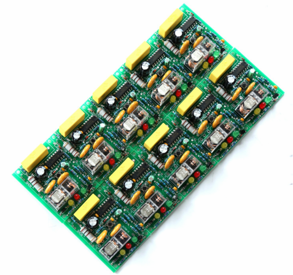
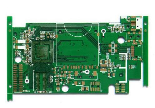
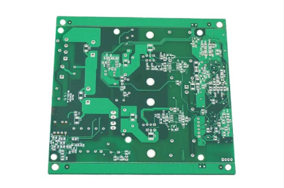
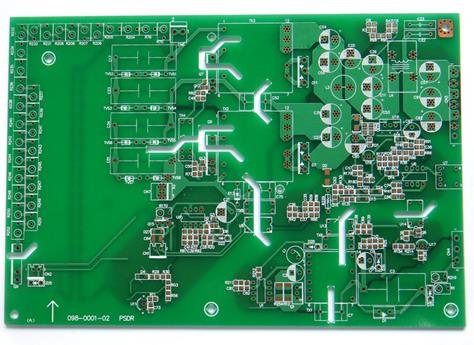
Solder mask plays a role in preventing welding and avoiding short circuits during welding. Solder mask forms a film attached to the board surface through silk screen printing, which is exposed to light and temperature, and undergoes curing.

A solder mask is a method of heating a workpiece to a molten or plastic state by utilizing the resistance thermal effect generated by the current flowing through the contact surface and adjacent areas, resulting in the formation of metal bonding. There are four main methods of solder masking, namely spot welding, seam welding, projection welding, and butt welding.
Solder masks can be divided into three types
1) Spot welding: Press the weldment tightly between two columnar electrodes, heat it with electricity, melt it at the contact point to form a molten nucleus, then cut off the electricity, and solidify and crystallize under pressure to form a densely structured solder joint. Spot welding is suitable for welding thin plates (overlapping) and steel bars below 4mm, and is widely used in the production of automobiles, airplanes, electronics, instruments, and daily necessities.
2) Seam welding: Seam welding is similar to spot welding, except that a rotating disc electrode is used instead of a cylindrical electrode. The stacked workpiece is pressurized and energized between the discs and is fed in with the rotation of the discs, forming a continuous weld seam.
Seam welding is suitable for overlapping thin plates with a thickness of less than 3 mm, and is mainly used in the production of sealed containers and pipelines.
3) Butt welding: According to different welding processes, butt welding can be divided into resistance butt welding and flash butt welding.
Reasons for PCB board solder mask
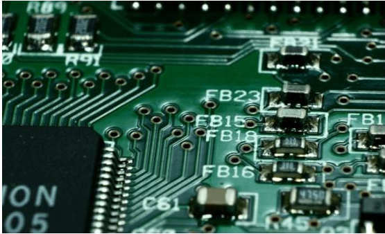
1. Preventing short circuits: There are many wires and pads on the PCB board, and if they are not properly isolated, they may cause short circuits. The solder mask layer can cover the area between the wire and the solder pad, reducing the risk of short circuits.
2. Prevention of leakage and electrical interference: If there is no appropriate isolation between wires or pads on the circuit board, it may cause interference and leakage of electrical signals. The solder mask layer provides electrical insulation, reducing the possibility of leakage and electrical interference.
3. Protection of circuit components: The solder mask layer can provide a layer of protection to prevent the components on the PCB surface from being eroded or damaged by external environments (such as dust, moisture, etc.). This helps to improve the reliability and lifespan of the circuit.
The Function of PCB solder-mask
1. Improve reliability: The solder mask layer can reduce the risk of short circuits, leakage, and electrical interference, thereby improving the reliability of the circuit. It ensures the stability and correct functionality of the circuit.
2. Improve welding quality: The presence of a solder mask layer can limit the diffusion of solder, making welding more precise and controllable. The welding pads on the solder pads and component pins are protected by a solder mask layer, which is not easily affected by external factors and improves the welding quality.
3. Convenient maintenance and debugging: The presence of a solder mask layer can provide clear circuit structure information, which is helpful for maintenance and debugging work. Through the solder mask layer, technicians can more easily identify circuit paths and connections, reducing errors and time.
Overall, in the PCB manufacturing process, a solder mask is applied to the surface of the PCB, covering the area between the metal wire and the solder pad. The solder mask layer on the PCB board plays a crucial role in protecting and optimizing circuit performance. It can improve the reliability of circuits, protect components, improve welding quality, and facilitate maintenance and debugging work.