The welding gap, also known as the butt gap, is the gap between two welded parts at the butt joint of the welded part. The size of the welding gap is directly related to the quality of the welded junction.

When the welding gap is too small, the weld seam is not easy to penetrate. When the welding gap is too large, it increases the difficulty of welding, and the large amount of filling affects the welding progress, increases the welding stress, and is prone to welding deformation.
Silkscreen, is also an ink and a solder mask is used to prevent ink (silkscreen) from covering. If the distance between the silkscreen and the solder mask is too close, it will lead to the loss of the silkscreen.
Generally, a spacing of around 30-40 millimeters is sufficient. The specific distance between welding points should be determined based on the specifications of the welded part, and it is not appropriate to be too dense or too thin.
The center distance between two adjacent butt welds on the pipeline:
For pipelines with a nominal diameter less than 150mm, it should not be less than the outer diameter and should not be less than 50mm;
For pipes with a nominal diameter equal to or greater than 150mm, they should not be less than 150mm.
If the spacing between welds is too small, the mechanical properties of the welded joints cannot meet the requirements of qualified pipelines, and leakage is prone to occur at the welded joints.
The Spacing Problem in PCB Design
1. Spacing between wires
It is recommended that the distance between the wiring and the wiring should not be less than 4 mils. The minimum line spacing is also the distance between lines and pads. The conventional 10mil is more common.
2. Pad aperture and pad width
If the aperture of the solder mask is mechanically drilled, the minimum should not be less than 0.2mm. If laser drilling is used, it is recommended that the minimum should not be less than 4mil. The aperture tolerance varies slightly depending on the plate, and can generally be controlled within 0.05mm. The minimum width of the welding pad should not be less than 0.2mm.
3. Spacing between pads
It is recommended that the spacing between pads should not be less than 0.2mm.
4. Distance between the copper sheet and plate edge
The distance between the charged copper sheet and the edge of the PCB board should preferably not be less than 0.3mm. If copper is laid on a large area, it is usually necessary to have an inward shrink distance from the board edge, usually set at 20mil.
5. Distance from silkscreen to solder mask
Screen printing is not allowed to cover the solder pad, as if the screen is covered with the solder mask, the screen area will not be able to be tinned during soldering, which will affect the installation of components.
It is generally required to reserve a spacing of 8mil. If it is because the area of some PCB boards is tight, it is barely acceptable for us to achieve a spacing of 4mil. If the silkscreen accidentally covers the solder pad during design, the silkscreen part left on the solder pad will be automatically eliminated during manufacturing to ensure tin on the solder pad.
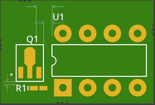
When we draw a silkscreenframe, we will make it slightly larger than the solder pad. Generally, the distance between the silkscreen frame and the edge of the solder pad is kept at about 6mil to ensure production and installation needs. If the drawing is too close, it will cause the silkscreen frame to be drawn on the solder mask. Generally, before production, CAM will remove the silk screen drawn on the solder mask to ensure the normal production of PCB boards and SMT chips in the later stage.