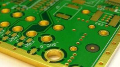
The solder mask layer is a PCB oil layer that covers copper wire and PCB material and is used for insulation and protection of the external PCB from short circuits and environmental influences. On the solder mask layer, you need to create openings (windows) to allow PCB pads to be soldered or connected, as well as some through holes that are not covered with PCB ink for heat dissipation. These openings on the solder mask layer are called solder mask openings.

In simple and easy-to-understand terms, a solder mask opening (window opening) removes the paint layer from the circuit, allowing the circuit to expose tin.
Why do we need to perform solder mask opening?
For via holes, if the window is not opened, the ink from the solder mask layer will enter the hole. For some holes that do not require ink to plug, they should be designed as through holes with windows. For components installed through holes, if the PCB is not soldered mask opening, the components cannot be soldered to the board normally. The aperture opening is not only convenient for welding but can also be measured on vias. To perform resistance welding and window opening on certain special positions of holes, a multimeter can be used to measure the through-hole.
Solder maks opening design
1. Dimensional design
In the PCB manufacturing process, the opening size of the solder mask layer should be larger than the desired exposed solder pad or copper area.
Due to the skin effect, PCB oil around the solder mask opening will accumulate and the exposed area will decrease. Usually, the width/length of the solder mask opening is 4mil larger than that of the solder pad.
Is it necessary to set the size of the solder to the mask opening during PCB design? No, you just need to maintain the same size as the required exposed solder pad/through-hole size, as the EDA tool will automatically expand the size of the solder mask opening.
2. Solder mask opening method for PCB solder mask layer
In PCB design, it can be set on the upper and lower solder mask layers.
Upper/lower solder green oil layer: The upper/lower solder green oil layer is used to prevent tin coating on copper foil and maintain insulation. It is possible to set solder mask green oil windows on this layer to access the solder pads, vias, and non-electrical traces on that layer.
1) In PCB design, the solder pad will default to open (OverRIDE: 0.1016mm), which means that the solder pad will expose copper foil and expand by 0.1016mm. During the wave soldering process, solder is soldered. It is recommended not to make any design changes to ensure solderability.
2) In PCB design, by default, a window (OverRIDE: 0.1016mm) will be opened for the through-hole, which means that the through-hole has exposed copper foil, expanded by 0.1016mm, and has wave soldering.
3) In addition, non-electrical wiring can also be carried out separately on this layer, which can block the green oil and open windows accordingly. If it is on copper foil wire, it is used to enhance the overcurrent capacity of the wire. Tin is added during the welding process.
The difference between solder mask opening and solder pad
1. Different uses
Solder mask opening is aimed at the solder mask layer, which is used to leave an area for welding or plug-in installation; The solder pad is aimed at the metal sheet area on the circuit board, used for welding with components.
2. Different meanings
Solder mask opening refers to the process of coating a layer of solder mask layer on the surface of a circuit board, and removing the solder mask layer in certain areas to leave areas for welding or plug-in installation; The solder pad refers to the metal circular or square area on the circuit board used for soldering with components, usually made of copper foil material.
Solder mask opening as a testing point for easy testing; Increase heat dissipation effect and facilitate heat dissipation; Tin can be added to it to increase the passing area of the current.