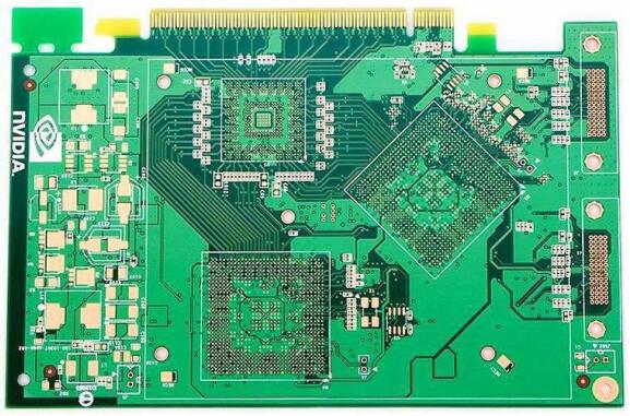
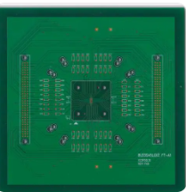
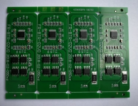
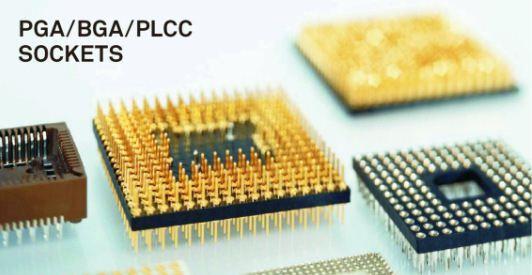
BGA is short for Ball Grid Array, which is a package of solder ball arrays. Its emergence stems from people's expectations for multifunctional, high-performance, compact, and lightweight electronic products. To achieve this goal, the market requires complex but small integrated circuit (IC) chips, which can ultimately increase packaging I/O density. Therefore, high-density and low-cost packaging methods are very necessary, and BGA is one of them.

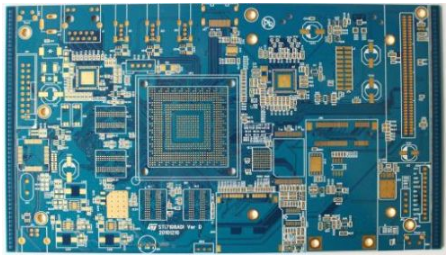
BGA is essentially a surface mount technology (SMT) or a surface mount packaging used for integrated circuits. Usually, traditional surface mount packaging uses the side of the package for connection to achieve a limited pin connection area. BGA packaging adopts a bottom connection, which can provide greater connection space, making the high density of PCB and the high performance of electronic products possible.
The advantages of BGA
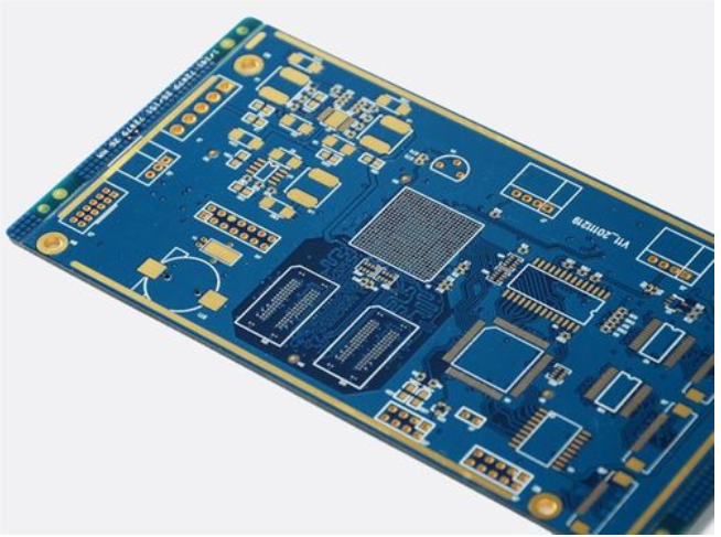
1. Efficiently utilize the space of the PCB. Using BGA packaging means less component involvement and a smaller footprint, which also helps to save space on custom PCBs, greatly improving the effectiveness of PCB space.
2. Improve thermal and electrical performance. Due to the small size of PCBs packaged with BGA, heat dissipation is easier. When the silicon wafer is installed at the top, most of the heat can be transferred downwards to the ball grid array. When installing a silicon wafer at the bottom, the back of the wafer is connected to the top of the package, which is considered one of the best ways to dissipate heat. The BGA package does not have pins that can be bent or broken, making it stable enough to ensure electrical performance on a large scale.
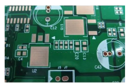
3. Improve the welding process and increase production yield. Most BGA packaging pads are relatively large, which makes large-area welding easy and convenient, thereby improving PCB manufacturing speed and improving manufacturing yield. The solder pads are large and easy to rework.
4. It causes minimal damage to the leads. The BGA lead wire is composed of solid solder balls, which are not easily damaged during use.
5. Reduce costs. All of the above advantages contribute to cost reduction. The efficient utilization of PCB space provides opportunities to save materials while improving thermal and electrical performance helping to ensure the quality of electronic components and reduce opportunities for defects.
BGA is a packaging method for integrated circuits using organic carriers. It has a reduced packaging area; Increased functionality and an increased number of pins; PCB board can self-center and easily solder during solution soldering; High reliability; Good electrical performance and low overall cost.