The most reliable PCB & PCBA custom service factory.
Language

Language
Smaller vias can be closer together, leading to a smaller PCB or freeing up space for additional components. Microvias have smaller aspect ratios than through-hole vias, and provide greater reliability for HDI PCB than other vias.
As the semiconductor and electronics market called for smaller, but higher function products, HDI PCB found its place in design engineers' arsenal. Shortening the distance between devices, or trace space, and using a large number of transistors translated to better performance in electronics.
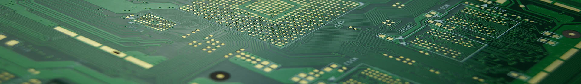
The current trend of electronic products: light, thin, short and small. Therefore, the required circuit density of the circuit board is getting smaller and smaller, and the design of blind and buried vias is increasing.
HDI (High Density Interconnection) PCB with via holes with a diameter of less than 6 mils are called microvias. Its most representative application is to realize PCB dielectric layer interconnection with buried vias and blind vias.
Advantages of HDI PCB
1. Reduce PCB cost (reduce the number of PCB layers).
2. Improve circuit density.
The greater the density of vias in a certain area, the greater the wiring paths in this area.
3. Promote the adoption of advanced assembly technology.
4. Better electrical performance and signal integrity.
5. Enhance reliability.
6. Improve thermal performance: HDI material has a thin dielectric layer and high Tg is beneficial to improve its thermal performance.
7. Improve RFI/EMI/ESD performance.
8. Improve layout efficiency.
HDI PCB micro-via metallization process
In the success of HDI production, the metallization of microvias is a key factor to ensure the conductivity of microvias and the reliability of the metal. The processes used to metalize the vias are as follows:
Electroless copper
Palladium-based direct metallization
Graphite method
Carbon ink technology
Conductive polymers
Electroless copper metallized microvia
Introduction of HDI PCB micro-hole plating process
Due to the micro-hole characteristics of the HDI board, the mass transfer effect in the hole is poor, so the plating difficulty in the hole is greater than that of the general through hole. In order to improve the quality of the electroplated layer in the hole, the following measures are mainly adopted:
Reduce current density and extend plating time.
Optimize plating solution parameters and plating bath meter.
Change vertical rack plating to horizontal rack plating.
Use reverse pulse plating instead.


