

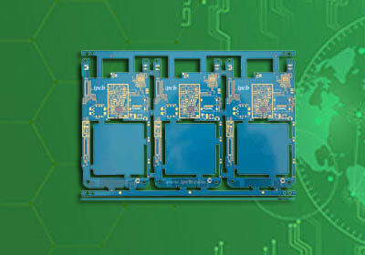


Model: HDI PCB
Layers: 4 layer - 48 layer
Material: Shengyi, Tuc, ITEQ, Panasonic
Construction: 1-5N, anylayer HDI PCB
Finished Thickness: 0.3 - 3.2mm
Copper Thickness: 0.5OZ/1OZ
Color: Green/White/Black/Red/Blue
Surface treatment: ENIG/OSP
Special technology: Gold thickness
Min Trace / Space: BGA 2mil/2mil
Application: HDI PCB circuit board
HDI PCB is High-Density Interconnector PCB, and HDI PCB is a type of PCB circuit board. Why is it called HDI printed circuit board? HDI PCB is a high density PCB, which has very small circuit space. The HDI PCB stack-up requires 0.1mm laser blind holes. This HDI microvia PCB requires HDI PCB manufacturer to have strong HDI PCB manufacturing process capabilities.
HDI PCB is widely used in smartphone motherboard PCB, server circuit board, POS motherboard, camera motherboard PCB, automobile circuit, Android smart motherboard, tablet PC motherboard, UAV controller, etc.
What is HDI PCB?
A PCB with buried blind holes is not necessarily an HDI PCB. HDI PCBs generally have blind holes and do not necessarily have buried holes. It depends on the level of HDI PCB your product is.
For example:
In the 6-layer HDI PCB, the first and second-order refer to the HDI circuit board requiring laser drilling, that is, the HDI circuit board.
6-layer first-order HDI PCB refers to blind holes: 1-2, 2-5, 5-6, i.e. laser drilling is required for 1-2, 5-6 That is, HDI PCB 1 n 1.
6-layer second-order HDI PCB refers to blind holes: 1-2, 2-3, 3-4, 4-5, 5-6 That is, laser drilling is required twice. First drill the embedded holes of 3-4, then press 2-5, then drill the laser holes of 2-3 and 4-5 for the first time, then press 1-6 for the second time, then drill the laser holes of 1-2 and 5-6 for the second time, and finally drill the via through-hole. It can be seen that the second-order HDI PCB has been pressed twice and laser-drilled twice. It becomes HDI PCB 2 N 2.
In addition, the second-order HDI PCB is also divided into staggered second-order HDI PCB and stacked second-order HDI PCB. Staggered second-order HDI PCB means that blind holes 1-2 and 2-3 are staggered, while stacked second-order HDI PCB means that blind holes 1-2 and 2-3 are stacked together, such as blind holes: 1-3, 3-4, 4-6.
And so on, HDI PCB 3 N 3, HDI PCB 4 N 4, HDI PCB 5 N 5, HDI PCB 6 N 6...

HDI PCB TYPE
Difference between HDI PCB vs standard PCB
HDI PCB is generally manufactured by the lamination method. The more times of lamination, the higher the technical grade of the PCB board. Ordinary HDI PCB board is basically one-time lamination, high-order HDI PCB adopts two or more lamination technologies and adopts advanced PCB technologies such as hole stacking, electroplating hole filling, laser direct drilling, and so on. When the density of PCB increases by more than eight layers, the manufacturing HDI PCB cost will be lower than the traditional complex pressing process.
The electrical performance and signal correctness of the HDI PCB is higher than those of standard PCB. In addition, the HDI PCB board has better improvement for radio frequency interference, electromagnetic wave interference, electrostatic discharge, heat conduction, etc. High-density integration (HDI) technology can make terminal product design more miniaturized and meet higher standards of electronic performance and efficiency.
HDI PCB is plated with blind holes and then pressed twice, which is divided into first-order (1+n+1), second-order(2+n+2), third-order(3+n+3), fourth-order(4+n+4), fifth-order(5+n+5), AnyLayerHDI PCB,etc.
The first-order is relatively simple, and the process and process are easy to control. The main problems of the second-order are alignment and punching and copper plating.
There are many kinds of second-order HDI PCB design. One is that each order is staggered. When it is necessary to connect the second adjacent layer, it is connected in the middle layer through wires, which is equivalent to two first-order HDI.
The second is that two first-order holes overlap, and the second-order is realized by superposition. The processing is also similar to two first-order holes, but there are many key process points to be specially controlled, that is, the above-mentioned.
The third method is to drill holes directly from the outer layer to the third layer (or n-2 layer). The process is different from the previous one, and the drilling is more difficult. For the third-order, the second-order analogy is used.

HDI PCB Stack-up
HDI PCB technology is the best choice for PCB designers when they need higher-density components.
1. In areas where the density of PCB components is high, HDI PCB uses micro-pores instead of through-holes.
HDI PCB via holes is used when higher precision holes are needed. Laser drilling micro-holes can be used up to a depth of about 0.1mm. Because the micropores have short cylinders, they will not be confronted with problems due to the different CT values of the substrates and copper. This is why micropores are more suitable than through-holes. For example, thin dielectric layers smaller than 0.005 inches are used to separate GND and PWR planes. This provides a low power impedance and can also be used to skip through holes from Layer 1 to Layer 3.
2. Improve HDI PCB wiring via hole.
In the design of the HDI PCB board, the rational layout of the holes is very important. These arrangements are designed to provide better signal integrity and improve the internal routing space.
3. Replace via hole with micropore.
Finer spacing BGA is increasingly complex for PCB design, and HDI PCB design rules provide space for interlaced and blind holes. For example, overlay a micropore on the through-hole or place a micropore on top of it. It can save more space for HDI PCB.
How to design HDI PCB stackup?
Although any PCB circuit board with a high number of layers will be expensive, these products have kept up with the trend of encapsulating more advanced functionality in a smaller space. With a 25um line width, HDI PCB designs are becoming smaller and smaller, and the limiting factors for wiring density are layers, net numbers, and a number of components. If you want to design advanced products to increase the limits of component and wiring density, be aware of the HDI PCB stacking before starting the HDI PCB layout.
How many layers are used in HDI PCB Layout? HDI PCB stacking and HDI PCB wiring is currently used in panels between 4 and 48 layers. The exact number of layers depends on the required line density, the total number of HDI networks, and the approximate amount of space they will occupy on the printed circuit board.
The process used to estimate the number of HDI PCB stack-up can be as follows:
1. Tracking size: First, you need to adjust the size of the route to the appropriate width and thickness to ensure impedance is controlled. Here, a preliminary layer thickness estimate is needed based on previous experience. Another way to do this is to look at the BGA spacing to set an upper limit on the line width and use this value to determine the layer thickness required for the desired line impedance.
2. Estimate of the net amount per layer: Once the required line width/layer thickness has been determined (and the spacing between differential pairs of routes) allows you to roughly determine how much space the signal layer will occupy within the HDI PCB layout area. This requires specifying an estimate of the HDI circuit board size; multiplying the approximate number of BGA breakthrough channels per unit area by the circuit board area will give you the number of each layer of the network. It can then be used to estimate the total number of layers required in the HDI PCB stack up.
3. HDI PCB Layer Count: Once you know the number of networks needed for each layer, simply divide your number of networks by this number to get a layer count. Note that this only gives you an estimate of the signal layers, not the total number of layers. Now, just add power and ground to your HDI PCB stack and you get an initial stack.

HDI PCB 2 n 2
Advantages of HDI PCB Board.
1. HDI PCB can reduce the cost of PCB, when the density of PCB increases by more than eight layers, the cost of manufacturing with PCB HDI will be lower than the traditional complex pressing process.
2. Increasing circuit density, the interconnection between traditional circuit boards and parts.
3. HDI PCB is conducive to the use of advanced construction technology.
4. HDI PCB better electrical performance and signal correctness
5. Good reliability
6. Can improve thermal properties
7. Improve radio frequency interference / electromagnetic wave interference / electrostatic discharge (RFI / EMI / ESD)
As with any other design, contact the HDI PCB manufacturer to ensure compliance with its HDI PCB guide (DFM) before creating an HDI PCB stackup or starting an HDI PCB layout. Many PCB manufacturers are highly focused on HDI PCB manufacturing and HDI PCB assembly, and they can make very thin, very dense cables that can hold many layers. Close communication with HDI PCB manufacturer can save manufacturing costs and ensure better HDI PCB fabrication.
IPCB is a professional china HDI PCB manufacturer. We offer high precision HDI PCB board fabrication and cheap HDI PCB. If you need an HDI PCB quotation, please send us an email.
Model: HDI PCB
Layers: 4 layer - 48 layer
Material: Shengyi, Tuc, ITEQ, Panasonic
Construction: 1-5N, anylayer HDI PCB
Finished Thickness: 0.3 - 3.2mm
Copper Thickness: 0.5OZ/1OZ
Color: Green/White/Black/Red/Blue
Surface treatment: ENIG/OSP
Special technology: Gold thickness
Min Trace / Space: BGA 2mil/2mil
Application: HDI PCB circuit board
For PCB technical problems, iPCB knowledgeable support team is here to help you with every step. You can also request PCB quotation here. Please contact E-mail sales@ipcb.com
We will respond very quickly.


