

HDI PCB is the abbreviation of High Density Interconnector Printed Circuit Board. HDI PCB is characterized by having very precise and small circuits. It usually needs to use 0.2mm buried holes and 0.1-0.05mm laser blind holes to conduct each layer of circuits.
According to the definition of the order of HDI PCB, every time a blind hole is made is counted as the first order of the HDI PCB. With the existing technology, one lamination is required for each order of the HDI PCB processed. The HDI circuit board with only blind holes in the inner layer means that after the first pressing, there is no need to make buried holes in the inner layer, only blind holes need to be made, and the circuits of other layers are connected by through holes and blind holes. For HDI circuit boards with only blind vias in the inner layer and designed for non-stacked vias, the blind vias in the inner layer do not need to be completely filled, but only need to be plated with enough copper for the blind vias. For HDI boards with stacked vias design , the blind holes in the inner layer must be completely filled.
HDI PCB is usually of symmetrical structure. We add a layer of laser blind holes on each side of it to order 1 (1+N+1, 2+N+2... n+N+n), There is a type of HDI PCB, which has no buried holes and only uses laser blind holes, that is Anylayer HDI PCB.
As shown in the figure below

Structure of HDI PCB
Blind hole manufacturing process of HDI PCB
1. When the blind hole is designed without stacking holes and the inner layer is completed with a copper thickness of 17.1 mm: inner layer patterning - pressing - browning - laser drilling - debrowning - copper sinking - whole board filling and electroplating - slicing Analysis - Inner Layer Patterning - Inner Layer Etching - Inner Layer AOI - Post Process.
2. Blind hole stacking design, and the inner layer is completed with a copper thickness of 17.1 mm: inner layer pattern production - pressing - browning - laser drilling - debrowning - copper sinking - whole board filling and electroplating - slice analysis - Copper reduction - inner layer patterning - inner layer etching - inner layer AOI - post process.
3. When the inner layer is completed with a copper thickness of 17.1 mm, the inner layered holes and non-stacked holes are designed, and the blind holes are made by filling and leveling: inner layer pattern production - browning - pressing - browning - laser drilling - debrowning - Copper Immersion - Hole Filling Electroplating - Slice Analysis - Inner Layer Pattern - Inner Layer Etching - Inner Layer AOI - Post Process.
It can be seen from the above analysis that when the inner layer blind hole is designed as a stacked hole, in order to ensure the filling of the blind hole, a larger filling parameter must be used to fill the blind hole, and then the surface copper should be reduced to the required thickness. Therefore, in the above three processes, the thickness of the surface copper is controlled according to the adjustment of the hole filling parameters. At present, the common hole filling processes include resin plug hole and electroplating hole filling. The resin plug hole is filled with epoxy resin by plating copper on the wall of the via hole, and finally copper plating on the surface of the resin, the effect is that the hole can be turned on. And there are no dents on the surface, which does not affect the welding. Electroplating fills the vias directly by electroplating, without voids, which is good for welding, but requires high process capabilities.

Manufacturing process of HDI PCB
HDI PCB manufacturing capacity of iPCB
Number of layers: 4-24 layers for mass production, 36 layers for samples
Minimum circuit width / spacing: mass production 2mil / 2mil (0.05mm / 0.05mm), sample 1.5mil/1.5mil (0.035mm / 0.035mm)
iPCB is a professional HDI PCB board manufacturer, we usually use electroplating to fill holes, if you have any HDI PCB questions, please do not hesitate to contact iPCB.
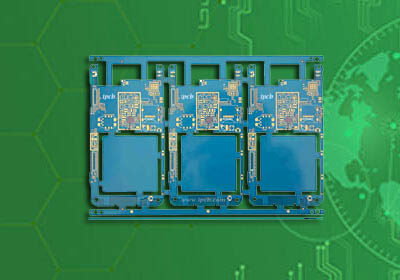
Smart Phone Main board PCB |
HDI PCB |
HDI PCB manufacturing |


