1: PCB thermal design Due to the relatively low temperature resistance and thermal conductivity of the printed circuit board substrate, the peel strength of the copper foil decreases as the working temperature increases. The operating temperature of the printed circuit board should generally not exceed 85°C.
When the motherboard structure is designed, the main heat dissipation methods are as follows: uniform distribution of heat load, installation of radiator components, strip-shaped heat conducting strips between the printed board and components, and local or global forced air cooling.
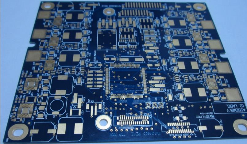
2: PCB vibration damping buffer design. Printed circuit boards are circuit components and device support components in electronic products, which provide electrical components between circuit components and equipment connections. In order to improve the vibration resistance and impact resistance of the printed circuit board, the load on the board should be reasonably distributed to avoid excessive stress.

For large and heavy parts (weights over 15g or over 27cm3), they should be arranged as close to the fixed end as possible, and their center of gravity or fixed metal structural parts should be lowered.
3: The anti-electromagnetic interference of the printed circuit board is to minimize the interaction and interference of the components on the printed circuit board. The components of the high-frequency circuit and the low-frequency circuit, and the high-potential and low-potential circuits should not be too close.
Input and output components should be as far away as possible, minimize the connection between high-frequency components, and minimize their distribution parameters and mutual electromagnetic interference. With the development of high-density fine line width/spacing, the spacing between wires is getting smaller and smaller, and the coupling and interference between wires and wires will bring spurious signals or error signals, commonly known as crosstalk or noise. This coupling effect can be divided into capacitive coupling and inductive coupling.
The spurious signals caused by these coupling effects should be reduced or eliminated through design or isolation:
1: When the signal wire and the ground wire are interlaced or the ground wire (layer) adopts a double-signal strip line, the adjacent double-layer signal
2: Surround the signal line to achieve a good isolation effect. The lines should not be placed in parallel, and should be perpendicular and inclined to each other to reduce the generation of distributed capacitors and prevent signal coupling. At the same time, it should not be a right-angled or acute-angled line, and a circular arc angle should be used to remove arcs and diagonal lines to minimize possible interference.
3: Reduce the length of the signal line. At present, the most effective way to shorten signal transmission lines under high-density lines is to adopt a multilayer board structure.
4: The highest frequency signal or the highest speed digital signal component should be as close as possible to the input and output (I/O) of the connection edge of the printed circuit board to make the transmission line wiring the shortest.
5: For the pins of high-frequency signal and high-speed digital PCB signal components, BGA (Ball Grid Array) type structure should be adopted, and the dense qfp (quad flat package) form should not be used as much as possible.
6: Using the latest CSP (bare chip packaging) technology.