The circuit board production process for ENIG surface treatment is as follows:
1. Front end tool data preparation
The first step to make a printed PCB bare board is to check whether the Gerber file design sent by the customer meets the standards that can be produced. Generally speaking, the PCB layout and its functional characteristics are designed by the customer, and the PCB board factory is only responsible for its production, so it is the same reason that there is often a gap between most designers and manufacturers. It is often found that the Gerber (Note 1) design files sent by customers cannot be achieved under current process capabilities. For example, the spacing between lines and lines, lines and holes, and holes and holes is too small, and it is easy to produce Cause a short circuit, or the line width is too thin, which may cause the circuit to be broken and cannot be produced. At this time, the board factory will generate the so-called engineering questionnaire EQ (Engineering Question) or DFM (Design For Manufacture) "Engineering Communication Article" and send it to the customer for confirmation, because In some places, it may be designed according to the special needs of customers. If you change it casually, it may cause the PCB to fail to meet the designer's expected requirements;
In addition, these engineering articles will also contain many engineering optimization suggestions, such as whether the solder mask between IC pins can be cancelled, whether some vias are covered with solder mask or copper plug holes, etc., before the communication is completed In a production step, each process condition of PCB production is disassembled from Gerber, such as each layer of wiring, solder mask, silk screen layer, surface treatment, and drilling materials, and then sent to the production line of each process for production. The follow-up will The process of these processes is described.
Note 1: The so-called Gerber is a general standard format that defines PCB production images. The content includes internal and external circuit layers, solder mask layers, silk screen layers, drilling layers, etc., which are somewhat similar to the IGS files or STEP files of the 3D design of the organization. For further information, please refer to Wikipedia's explanation of Gerber.
2. Preparing the phototools (circuit board negative output)

Under the control of temperature and humidity, use a laser film plotter to draw the film of the circuit board. These film will be used as a mask for the image exposure of each layer of the circuit in the subsequent circuit board manufacturing process. The solder green paint process also needs to use a film. In order to ensure the correctness of the X-Y relative position of each layer of the circuit, a laser will be used to perforate each film for the subsequent positioning of different circuit layers.
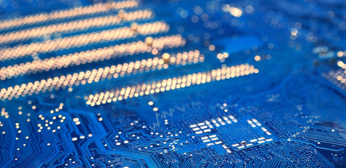
This kind of film is actually a transparent PET material with a black image printed on it. It is similar to the earlier stuff that used a paper-like projection film on the projector. Now it has been completely replaced by a digital projector. Young people probably don’t know this stuff. .
3PCB inner layer circuit molding
Pickling and cleaning of copper surface 》Roughening of copper surface 》Pressing dry film 》Inner layer exposure 》Development
The inner layer structure of multi-layer circuit boards (more than four layers) is usually made of a whole piece of CCL (Copper Clad Laminate) Note 2 as the material. Most of the CCL is based on resin and reinforcing materials. The substrate is covered with a whole piece of copper foil. In the film, the operator takes the CCL. After taking it, the surface of the copper foil will be cleaned by pickling to ensure that there is no other dust or impurities. Above, as long as there is any small amount of foreign matter, it will affect the subsequent lines.
Then mechanical grinding will be used to roughen the surface of the copper foil to enhance the adhesion of the dry film to the copper foil, and then a layer of dry film will be coated on the surface of the copper foil. Paste an inner circuit film on both sides of the CCL and set it up on the exposure machine. Use positioning holes and vacuum to tightly fit the film and CCL, and use ultraviolet light in the yellow light area to make the film unavailable. The dry film in the shaded area is chemically changed and cured on the CCL. Finally, the unexposed dry film is removed with a developer solution. At this time, the black seen in the film is to wash away the remaining exposed dry film, pay attention to here The "negative film" is used, and the other areas showing the copper surface will be etched away in the later process.
Development means to use a developer to remove the unexposed dry film and leave only the required part.
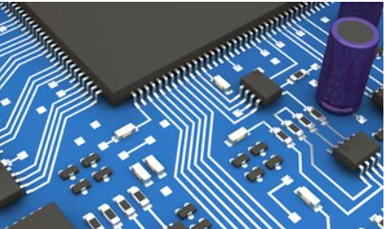
The core of the PCB material is the base plate. The PCB base plate is composed of resin, reinforcing material and copper foil. The most common substrate is CCL. Copper foil substrates are divided into three categories according to the material of the base material. They are paper substrates, composite substrates and FR-4 substrates. Their characteristics and uses are also different. Among them, FR-4 is the current mainstream. FR-4 substrates are commonly used in computer components and peripheral equipment. For example, the printed circuit boards used in products such as motherboards and hard disk drives are made from FR-4 substrates.