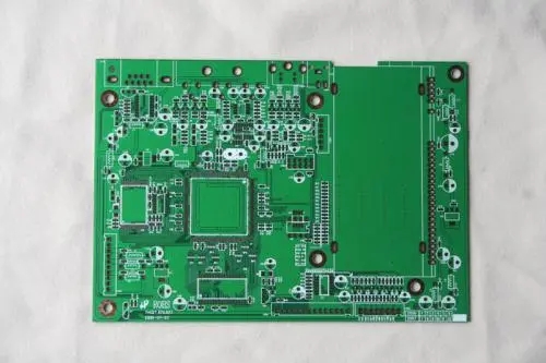
The PCB design process based on signal integrity computer analysis is shown in Figure 2. Compared with the traditional PCB design method, the design method based on signal integrity analysis has the following characteristics:

Before PCB board design, first establish a signal integrity model for high-speed digital signal transmission.
According to the SI model, a series of pre-analysis of the signal integrity problem is carried out, and the appropriate component types, parameters and circuit topology are selected according to the results of the simulation calculation as the basis for the circuit design.
In the circuit design process, the design plan is sent to the SI model for signal integrity analysis, and the tolerance range of the components and PCB board parameters, the possible topological structure and parameter changes in the PCB layout design, etc., are calculated and analyzed. Solution space.
After the circuit design is completed, each high-speed digital signal should have a continuous and achievable solution space. That is, when the PCB and component parameters change within a certain range, the layout of the components on the PCB board and the wiring of the signal lines on the PCB board have a certain degree of flexibility, the requirements for signal integrity can still be guaranteed .
Before the PCB layout design starts, the boundary value of each signal solution space obtained is used as the constraint condition of the layout design, which is used as the basis for the design of the PCB layout layout and wiring.
In the PCB layout design process, the partially completed or fully completed design is sent back to the SI model for post-design signal integrity analysis to confirm whether the actual layout design meets the expected signal integrity requirements. If the simulation results cannot meet the requirements, you need to modify the layout design and even the circuit design, which can reduce the risk of product failure due to improper design.
After the PCB design is completed, the PCB board can be made. The tolerance range of the PCB board manufacturing parameters should be within the range of the solution space of the signal integrity analysis.
After the PCB board is manufactured, the instrument is used for measurement and debugging to verify the correctness of the SI model and SI analysis, and use this as the basis for correcting the model.
On the basis of the correct SI model and analysis method, usually the PCB board can be finalized without or only a few repeated modifications to the design and production, which can shorten the product development cycle and reduce the development cost.