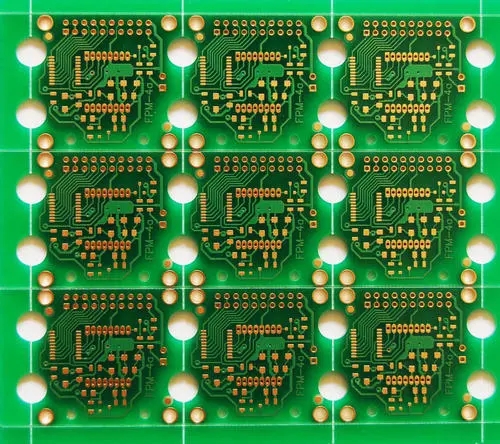
Precautions for via design in PCB
1. Considering the cost and signal quality, choose a reasonable size via size. For example, for the 6-10 layer memory module PCB design, it is better to use 10/20Mil (drilled/pad) vias. For some high-density small-size boards, you can also try to use 8/18Mil. hole. Under current technical conditions, it is difficult to use smaller vias. For power or ground vias, you can consider using a larger size to reduce impedance.

2. The two formulas discussed above can be concluded that using a thinner PCB is beneficial to reduce the two parasitic parameters of vias.
3. Try not to change the layers of the signal traces on the PCB board, that is to say, try not to use unnecessary vias.
4. The power and ground pins should be drilled nearby, and the lead between the via and the pin should be as short as possible, because they will increase the inductance. At the same time, the power and ground leads should be as thick as possible to reduce impedance.
5. Place some grounded vias near the vias of the signal layer to provide the nearest loop for the signal. It is even possible to place a large number of redundant ground vias on the PCB board. Of course, the design needs to be flexible. The via model discussed earlier is the case where there are pads on each layer. Sometimes, we can reduce or even remove the pads of some layers. Especially when the density of vias is very high, it may lead to the formation of a break groove that separates the loop in the copper layer. To solve this problem, in addition to moving the position of the via, we can also consider placing the via on the copper layer. Reduced pad size
PCB design output knowledge
The PCB design can be exported to a printer or a gerber file. The printer can print the PCB in layers, which is convenient for designers and reviewers to check; the gerber file is handed over to the board manufacturer to produce the printed board. The output of the gerber file is very important. It is related to the success or failure of this design. The following will focus on the matters needing attention when outputting the gerber file.
a. The layers that need to be output are wiring layers (including top layer, bottom layer, middle wiring layer), power layer (including VCC layer and GND layer), silk screen layer (including top silk screen, bottom silk screen), solder mask layer (including top solder mask) And bottom layer solder mask), and also generate a drilling file (NC Drill)
b. If the power layer is set to Split/Mixed, then select Routing in the Document item of the Add Document window, and each time the gerber file is output, you must use Pour Manager's Plane Connect for copper pour on the PCB diagram; if it is set to CAM Plane, select Plane. When setting the Layer item, add Layer25, and select Pads and Vias in Layer25
c. In the device setup window (press Device Setup), change the value of Aperture to 199
d. When setting the Layer of each layer, select the Board Outline
e. When setting the Layer of the silk screen layer, do not select Part Type, select the top layer (bottom layer) and Outline, Text, Line of the silk screen layer
f. When setting the layer of the solder mask layer, select vias to indicate that no solder mask is added to the vias, and not to select vias to indicate solder masks, depending on the specific situation.
g. When generating drilling files, use the default settings of PowerPCB and do not make any changes
h. After all the gerbera files are output, open and print them with CAM350, and check them by the designer and reviewer according to the "PCB checklist"