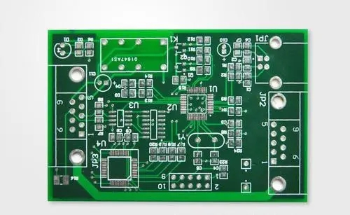
The type of PCB distinguishes, single-sided, double-sided and multi-layer PCB boards
According to different types, PCBs are roughly divided into: single-sided, double-sided and multi-layer boards.

The single panel design is relatively simple, the parts are concentrated on one side, and the wires are concentrated on the other side. Because the wires only appear on one side, we call this kind of PCB a single-sided board. Because single-sided boards have many strict restrictions on the design of the circuit (because there is only one side, the wiring cannot cross and must go around a separate path), only the early circuits and the relatively simple circuit boards (such as TV boards) are used This kind of PCB design.
There are wiring on both sides of the double panel. However, to use wires on both sides, there must be a proper circuit connection between the two sides. This kind of "bridge" between circuits is called a via (Via). A via is a small hole filled or plated with metal on the PCB, which can be connected to the wires on both sides. Because the area of the double-sided board is twice as large as that of the single-sided board, and because the wiring can be interleaved with each other, it is more suitable for use in circuits that are more complicated than the single-sided board.
As the PCB board area is getting smaller and smaller, and the signal rise time is getting shorter and shorter. In order to increase the area that can be routed and improve the performance of the product, most IT products in the industry today use multi-layer board design. Sheet double-sided boards, and put a layer of insulating layer between each board and stick it firmly (press-fitting).
The number of layers of the board means that there are several independent electrical layers. Usually the number of layers is even and contains the two outermost layers. Because the layers in the PCB are tightly integrated, it is generally not easy to see the actual number of layers; to identify the PCB, the PCB board can be exposed to the light. If you can see the transparent dividing line, then this PCB is made of 4-layer PCB. For PCBs with 6 layers and above, most PCB board designers will etch the signs of each layer on each layer of the PCB. We can clearly see these signs to the light to identify how many layers of PCB design are used.
Just mentioned the concept of "Via" in the double-sided board. Similarly, in the multi-layer PCB, "Via" is also used to connect the bridge between layers. However, VIA in a multilayer PCB includes through holes, buried holes and blind holes. The through holes penetrate the entire PCB. The advantages are convenient production and low cost. However, as the PCB space is getting smaller and smaller today, the waste of through holes has nothing to do with others. The shortcomings of the circuit space of the layer are very obvious. Therefore, we use the blind buried via process. Blind vias are used to realize the interconnection between the surface PCB and the inner PCB without penetrating the entire PCB; while the buried vias are only realized between the inner PCBs. The interconnection does not affect the surface space. These two via processes basically solve the shortcoming of the via hole wasting space, but the cost is relatively high.
[color=#FF69B4] [Note] Via (via): In order to connect the lines between the layers, drill a common hole at the Wenhui of the wires that need to be connected on each layer. This is the via. In the process, a layer of metal is plated on the cylindrical surface of the hole wall of the via by chemical deposition to connect the copper foil that needs to be connected to the middle layers, and the upper and lower sides of the via are made into ordinary pad shapes, which can be directly It is connected to the upper and lower lines, or not connected.