The skills and methods for high-frequency PCB design are as follows:

1. The corner of the transmission line should be 45° to reduce the return loss (Figure 1);
2. Use high-performance insulated circuit boards whose insulation constant values are strictly controlled by level. This method is conducive to effective management of the electromagnetic field between the insulating material and the adjacent wiring.
3. To improve the PCB design specifications related to high-precision etching. It is necessary to consider that the total error of the specified line width is +/-0.0007 inches, the undercut and cross-section of the wiring shape should be managed, and the plating conditions of the wiring side wall should be specified. The overall management of wiring (wire) geometry and coating surface is very important to solve the skin effect problem related to microwave frequency and realize these specifications.
4. The protruding leads have tap inductance, so avoid using components with leads. In high frequency environments, it is best to use surface mount components.
5. For signal vias, avoid using a via processing (pth) process on sensitive boards, because this process will cause lead inductance at the vias. For example, when a via on a 20-layer board is used to connect layers 1 to 3, the lead inductance can affect layers 4 to 19.
6. To provide a rich ground plane. Use molded holes to connect these ground planes to prevent the 3D electromagnetic field from affecting the circuit board.
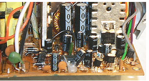
7. To choose electroless nickel plating or immersion gold plating process, do not use HASL method for electroplating. This kind of electroplated surface can provide better skin effect for high frequency current (Figure 2). In addition, this highly solderable coating requires fewer leads, which helps reduce environmental pollution.
8. The solder mask can prevent the flow of solder paste. However, due to the uncertainty of the thickness and the unknown of the insulation performance, the entire surface of the board is covered with solder mask material, which will cause a large change in the electromagnetic energy in the microstrip design. Generally, a solder dam is used as the solder mask.
If you are not familiar with these methods, you can consult an experienced design engineer who has been engaged in military microwave circuit board design. You can also discuss with them the price range you can afford. For example, copper-backed coplanar microstrip design is more economical than stripline design. You can discuss this with them to get better suggestions. Good engineers may not be accustomed to considering cost issues, but their suggestions are also quite helpful. Now try to train young engineers who are unfamiliar with RF effects and lack experience in handling RF effects. This will be a long-term job.
In addition, other solutions can also be adopted, such as improving the computer type to enable it to handle RF effects.
The above is the introduction of the method of interconnection in the PCB board. Ipcb is also provided to PCB manufacturers and PCB manufacturing technology.