1. In the switching power supply high voltage board, the high voltage and large current signals are completely separated from the low voltage and small current weak signals.

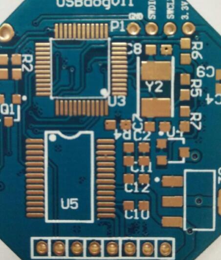
2. In high-frequency digital circuits, crystals and crystal oscillators must be placed close to the chip. The output capacity of the crystal oscillator also has a certain limit. If the crystal oscillator is too far away from the chip layout, the square wave signal output by the chip after receiving the crystal signal will be interfered to a certain extent, and it will not be a fixed frequency to a certain extent., This will cause the digital circuit to be unable to work synchronously.
3. Circuits with the same module and structure adopt a "symmetrical" layout, and the quick layout method can use the module reuse function in the PCB design software.
4. The arrangement of components needs to be considered for later debugging and maintenance, that is, do not place large components around small components; there must be enough space around components that need to be debugged.
5. The decoupling capacitor is close to the IC power supply pin, and the loop formed between it and the power supply and ground is the shortest.
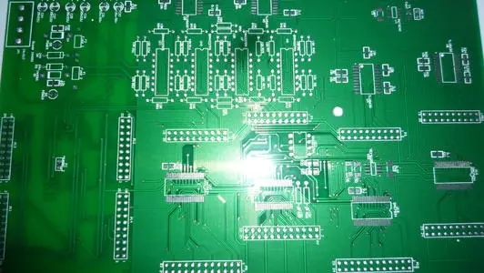
PCB wiring specification details
1. Cross-segmentation: Refers to the signal reference plane is not continuous, the signal line spans two different reference planes, and a series of EMI and crosstalk are generated to the signal. The cross-segmentation in PCB boardmay not have a great impact on low-frequency signals, but for some high-frequency digital circuits, it is very important to avoid cross-segmentation.
2. Pad wire problem: In PCB design, pad wire is also a detail that needs attention. If the two solder pads of the 0402 resistor package are routed diagonally, plus the solder mask deviation caused by the PCB production accuracy (the solder mask window is 0.1mm larger than the solder pad on one side), the result will be as shown in the left picture below. Pad. In this case, due to the effect of the surface tension of the solder during resistance welding, there will be a bad rotation as shown in the right picture below.
Adopt a reasonable wiring method, and the pad connection adopts a fan-out method that is symmetric about the long axis, which can effectively reduce the bad rotation after the CHIP component is mounted. If the fan-out line of the pad is also symmetrical about the short axis, the drift of the CHIP component after mounting can also be reduced.
And the adjacent network cannot be directly connected to the same network. You need to connect the pads before connecting. As shown in the figure, the straight chain is easy to cause continuous welding during manual welding.
3. Details of equal length in the differential trace pair
Compared with ordinary single-ended signal routing, the most obvious advantage of differential signal is its strong anti-interference ability, effective suppression of EMI, and accurate timing positioning. Many designers believe that maintaining equal spacing is more important than matching the length of the line. The most important rule in the design of PCB differential traces is to match the line length. Other rules can be based on it, and the design can be handled flexibly according to the actual application. The following figure lists some detailed methods of internal equal length.
4. Clock signals and high-frequency signals should be shielded as far as possible. If there is no space to cover the ground, try to separate the space of 3W.
5. When wiring and punching holes, you need to pay attention to the splitting of the reference plane of the adjacent layer. Such a split will cause the signal transmission path to be too long. It is better to keep a distance between the holes and the holes that can pass a line, so as to prevent the plane layer from being cut. Affect the integrity of the reference plane.
Production details in PCB design
1. The details of the golden finger window opening: I believe everyone has known about the golden finger window. During the design process, you must pay attention to this small detail of the golden finger window opening. The golden finger area must be fully opened. Some designers When packaging, the window area will be added to prevent forgetting to add it in the PCB later. Of course, some careless engineers will forget this small detail, resulting in a huge discount in the performance and service life of the product after the PCB is produced.
Among them, the processing method of opening the window in the PCB: draw the window area in the solder mask area corresponding to the gold finger, which can be drawn with copper or 2D lines.
The role of golden finger window opening: golden finger window opening means that there is no green oil between the device pad and the pad, so as to avoid long-term plugging and plugging and causing the green oil to fall off, thereby affecting the performance and quality of the product.
Device pad tombstone phenomenon: This detail involves the PCB packaging design, and it is also a little bit related to the method of pad wiring introduced to you before. PCB packaging is also very important for PCB design. The packaging on the PCB board is the mapping of the actual device, so when designing the package, it must be noted that the pad design should strictly maintain symmetry, and the design size should not be too different from the actual size. .
For example, for resistance-capacitance packaging, the pads on both sides need to be symmetrical and have the same size to ensure that when the solder melts, the surface tension of all solder joints on the components can be balanced, and ideal solder joints have been formed. The pad is asymmetrical. During reflow soldering, the solder on the larger end of the pad cannot achieve the desired melting and wetting effect, causing the device to shift and tombstone this phenomenon.