


A 20-layer PCB is a multi-layer printed circuit board with 20-layers of copper, alternating with a substrate called epoxy resin. Some of the main materials useful in manufacturing 20 layer PCBs include wire mesh, substrate, solder mask, and copper.
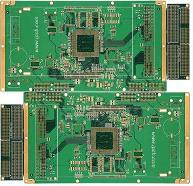
20 layer PCB
Application of 20-layer PCB
1. Consumer electronics
The 20-layer circuit board is very useful in manufacturing electronic products commonly used in offices or homes. These products include calculators, music players, watches, smartphones, and more. It can also be used to manufacture electric kettles, washing machines, LED light bulbs, and kitchen appliances.
2. Communication electronic products
The 20-layer PCB is very useful in the manufacturing of GPRS, radar electronics, communication towers, computer servers, and satellites. Other applications that use a 20-layer PCB include LNA, filters, mixers, power amplifiers, sonar antennas, phase-locked loops, and attenuators.
3. Computer
The 20-layer PCB is very useful in the production of computers and other components such as power supplies, graphics cards, EEPROMs, and motherboards. Others include ADCs, computer mice, keyboards, and circuits for image processing.
4. Automation
Operations carried out in the industry are usually susceptible to pressure, dust, temperature, humidity, and impact, which is why 20-layer PCBs are very reliable. In addition, different industrial applications such as automotive manufacturing, robotics, and conveyor belts all use this type of PCB.
5. Medical equipment
The 20-layer PCB is very useful in the testing and monitoring of medical devices. In addition, the 20-layer PCB can be used for blood pressure measurement devices, devices for monitoring infrared temperature, electronic machines for sugar testing, etc.
6. National Defense, Aerospace, and Military
The 20-layer circuit board is a useful military machine, such as surveillance, radar, and unarmed ground and air vehicles. In addition, they are also useful for railguns, navigation systems, artificial intelligence, and automatic artillery.
Layered structure of a 20-layer PCB
20-layer PCB stacking refers to the formation of 20-layers of insulation and copper layers into a printed circuit board before the layout of the circuit board.
These overlays play an important role in reducing the vulnerability of circuits to external noise. In addition, the crosstalk, impedance, and radiation issues that occur in high-speed printed circuit board layers can be alleviated by stacking.
The manufacturing process of 20-layer PCB
1. Imaging Process
Here, you can achieve digital design on the circuit board. Next, it will be transferred from your software to your circuit board.
2. Etching process
This process involves removing excess metal from printed circuit boards using industrial solvents.
3. Pressing
Here, with a Tablet press, you can combine 20 layers of PCB. In the end, you generated aboard.
4. Machining
In the process of processing this type of printed circuit board, you need to drill through holes and holes. This drilling ensures the connection between all layers of the PCB.
5. Plating
During the manufacturing process, you apply metal to complete through and through holes.
Manufacturing steps for a 20-layer PCB
1. The first step is to analyze the requirements of the circuit board and then select the components of the printed circuit board.
2. Secondly, design the front end within the system
3. Next, is the initialization of the photo tool. You can achieve this by transferring software images to printed circuit boards.
4. The fourth is the printing of the inner layer of the PCB
5. The next step is to remove excess copper from your board by etching
6. The sixth step involves aligning the inner layers of the PCB. You can do this by punching in registration.
7. Finally, perform an optical inspection of the printed circuit board you have completed.
Design Specification for 20 Layer PCB
1. PCB must operate at high speed and also have high capacity
2. Its heat resistance must be excellent
3. This type of PCB must be the ideal choice for manufacturing powerful, portable, and even small devices
4. There must be an alternating layer of 20 copper substrates
Advantages of 20-layer PCB
1. The assembly density is high, the volume is small, and the weight is light, meeting the needs of the miniaturization of electronic equipment.
2. Due to the high assembly density, the wiring between various components (including components) is reduced, installation is simple, and reliability is high.
3. Due to the repeatability and consistency of graphics, errors in wiring and assembly are reduced, and equipment maintenance, debugging, and inspection time is saved.
4. It can increase the number of wiring layers, thereby increasing design flexibility.
5. It can form circuits with a certain impedance and form high-speed transmission circuits.
6. Circuit and magnetic shielding layers can be set, and metal-core heat dissipation layers can also be set to meet special functional needs such as shielding and heat dissipation.
The 20-layer PCB has been widely used in the production and manufacturing of electronic products due to its flexible design, stable and reliable electrical performance, and superior economic performance.
With the continuous development of electronic technology and the increasing requirements for electronic equipment in industries such as computers, healthcare, and aviation, circuit boards are developing in the direction of reduced volume, reduced quality, and increased density. Due to the limitations of available space, it is no longer possible to further improve the assembly density of single and double-sided printed boards. Therefore, it is necessary to consider using multi-layer circuit boards with higher layers and assembly density.


