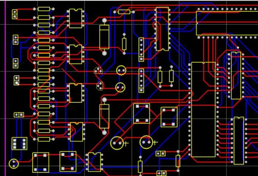
A circuit diagram, also known as a PCB schematic, is a graphical representation of the components required to make a circuit board. The schematic also indicates the location of these components on the circuit board, as well as all other aspects of the circuit design that connect the circuit board.

Circuit diagram
A circuit diagram is a diagram that uses circuit component symbols to represent circuit connections. A circuit diagram is a schematic layout diagram that represents the composition and relationship of various components using standardized physical and electrical symbols for research and engineering planning purposes. The working principle between components can be obtained from the circuit diagram, providing a planning solution for analyzing performance, and installing electronic and electrical products. In the design of the circuit, engineers can leisurely perform it on paper or computer, and confirm its completeness before proceeding with actual installation. Improve and fix errors through debugging until successful.
Composition of circuit diagram
The circuit diagram mainly consists of four parts: component symbols, wiring, nodes, and annotations.
1. The component symbol represents the component in the actual circuit, and its shape is not necessarily similar or even completely different from the actual component. But it generally represents the characteristics of the component, and the number of pins is consistent with the actual component.
2. Wiring represents the actual wires in a circuit. Although it is a single wire in the schematic, it is often not a wire but various shapes of copper foil blocks in commonly used printed circuit boards, just like many wiring in radio circuit diagrams may not necessarily be linear in printed circuit board diagrams, but can also be copper films of certain shapes.
3. Nodes represent the connection relationship between several component pins or wires. All component pins and wires connected to nodes, regardless of their number, are conductive.
4. Annotations are very important in circuit diagrams, and all text in the circuit diagram can be classified as annotations. Upon closer inspection of the above diagrams, it can be seen that there are annotations in various parts of the circuit diagram, which are used to indicate the model, name, and so on of the components.
How to convert a circuit diagram to PCB?
1. Firstly, design a schematic diagram according to the requirements of the project, which includes how to route the circuit and which electronic components to use.
2. Next is to use circuit diagram software, such as Protel or PADS, to draw PCB boards according to the schematic diagram. The drawing board actually involves packaging and arranging these components and connecting them online.
3. The next step is to provide the drawings to the PCB manufacturer. Firstly, cut a large piece of board into small pieces that meet the requirements based on the size of the circuit board.
4. Punching refers to some screw holes, some fixed installation holes, etc.
5. After copper deposition, electroplating, film removal, etching, green oil, screen printing of characters, forming, testing, and other processes, a PCB board can be obtained.
In theory, it is also possible to correspond the circuit diagram to the components on the PCB board, but the specific difficulty mainly depends on factors such as component type, component quantity, and PCB board layout. If there are few components, a small quantity, and a relatively simple circuit, then by observing the position, pins, and solder joints of each component on the PCB board, you can try to manually draw the corresponding schematic diagram, but you need to have a certain understanding of the basic knowledge of the components and circuit principles. For PCB boards with complex circuits, to avoid misunderstandings and misunderstandings, it is best to combine relevant information of the PCB board (such as schematic diagrams, layout diagrams, descriptions, BOM tables, etc.), and then compare and analyze them comprehensively. In addition, there are many automated circuit analysis software on the market now, which automatically generate corresponding schematic diagrams by scanning PCB boards. This method can achieve faster and more accurate conversion between PCB boards and schematic diagrams. Overall, it is theoretically possible to generate schematic diagrams based on the components on the PCB board, but it requires a certain level of knowledge and ability. For PCB boards with complex circuits, it is best to combine other methods for analysis.
Using circuit diagram simulation software for circuit-aided design and virtual circuit experiments can improve engineers' work efficiency, save learning time, and make physical diagrams more intuitive.