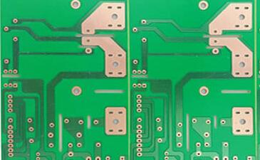
A double-sided PCB board prototype is a substrate covered by two layers of copper foil circuits, separated by insulating materials in the middle. Among them, conductive holes are processed through methods such as drilling or chemical etching to achieve the connection and crossing of circuits on both sides, thereby achieving circuit functions.

Both sides of the PCB double-sided pcb board prototype have wiring. However, to use wires on both sides, it is necessary to have appropriate circuit connections between the two sides. The bridge between these circuits is called a guide hole. A guide hole is a small hole filled or coated with metal on a PCB that can be connected to wires on both sides. Because the area of a double-sided PCB board prototype is twice that of a single panel, and because the wiring can be interleaved and wound to the other side, it is more suitable for use in more complex circuits than a single panel.
A double-sided PCB board prototype is a very important type of PCB board in the circuit board market. There are double-sided circuit board prototypes with metal bases, Hi Tg heavy copper foil circuit boards, flat and winding double-sided circuit boards, high-frequency PCBs, mixed dielectric base high-frequency double-sided pcb board prototypes, etc. It is suitable for a wide range of high-tech industries such as telecommunications, power supply, computers, industrial control, digital products, scientific and educational instruments, medical equipment, automobiles, aerospace defense, etc.
A double panel is a printed circuit board that includes both the top and bottom layers, with copper coated on both sides. Both sides can be wired and soldered, and there is an insulation layer in the middle. It is a commonly used type of printed circuit board. Both sides can be wired, greatly reducing the difficulty of wiring, so it is widely adopted.
The difference between single-side PCB board and double-side PCB board prototype
Single panel refers to a single-sided circuit board, with components on one side and wires on the other side; a double-sided PCB board prototype can be used to lay components and wiring on both sides. Because a single panel only has one side and cannot be crossed, the wiring difficulty is relatively high, while a double-sided panel can be wired on both sides, making it less difficult and more suitable for use in complex circuits. The production process of a double-sided PCB board prototype is more difficult than that of single panels, mainly because the top and bottom layers of copper-clad panels require through-hole connections and wiring.
The difference between single-side pcb board and double-side PCB board prototypes is reflected in the following points
1. Process: Single-side pcb welding is concentrated on one side, and components are placed on the other side; Both sides of the dual panel can be welded, allowing for both surface-mounted components and connectors.
2. Material: A single panel only has copper foil on one side, while a double-sided PCB board prototype has copper foil wiring on both sides, and the copper foils on both sides are connected through vias.
3. In terms of the production process:
1) Production process of single panel:
Material cutting → drilling positioning → Silk screen circuit → Etching → Silk Screen text, curing → mold punching and cutting appearance → Circuit inspection and testing → Packaging and shipping
2) The production process of double-sided boards:
Cutting → Drilling → Copper Deposition → Pattern Transfer → Pattern Electroplating → Etching → Tin Removal Cleaning → Resistance Welding → Screen Printing → Mold Punching and Cutting Appearance → Inspection and Testing → Packaging and Shipping
Although there are some differences between single side pcb board and double-sided PCB board prototypes, their structures are the same, including solder pads, vias, mounting holes, connectors, electronic components, wires, fillers, and electrical boundaries.
The working level is also the same, whether it is a single panel or a double-sided PCB board prototype, there are many types of working levels, such as a signal layer, silk screen layer, solder mask layer, solder paste layer, grounding layer, etc. Usually, a circuit board has dozens of signal layers, which are used to store components related to signals. The top layer contains components, the bottom layer contains copper, and the middle layer contains signal wiring; The silkscreen layer is used to draw the appearance of components and print product numbers, component models, company names, etc; The solder barrier layer is used to prevent the flow of solder and prevent areas that do not require soldering from getting contaminated with solder, causing short circuits in other components; The function of the solder paste layer is to paste SMD components onto the circuit board for easy soldering; The grounding layer connects the copper film of the ground wire layer to the ground wire pin.
The double-sided PCB board prototype is an important electronic component with excellent performance and a wide range of applications. Having a higher signal transmission rate; More reliable circuit connection; Larger usable area; More convenient for wiring and debugging.