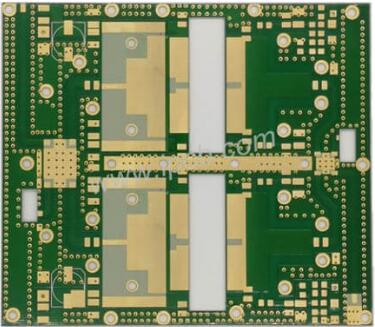
ENIG plating process is a surface treatment process used in PCB manufacturing. Its full name is the ENIG electroplating process, which forms a metal protective layer by electroplating a mixture of nickel and metal onto the Copper substrate. This protective layer can be used to protect circuit boards from chemical properties such as oxidation and corrosion.

ENIG, also known as electroplated nickel gold, deposited nickel gold, or electroless nickel gold, is a chemical reaction that replaces palladium on the surface of copper, then deposits a layer of nickel-phosphorus alloy on top of the palladium core, and then deposits a layer of gold on the surface of nickel through the substitution reaction.
The Function of PCB ENIG Plating
1. The copper on the circuit board is mainly red, and the copper solder joints are prone to oxidation in the air, which can form poor conductivity or poor contact, reducing the performance of the circuit board. Therefore, it is necessary to perform surface treatment on the copper solder joints. The deposition of gold is to plating gold on them, which can effectively isolate the copper metal and air to prevent oxidation. Therefore, the deposition of gold is a treatment method for surface oxidation prevention, It is a chemical reaction that covers the surface of copper with a layer of gold, also known as gold plating.
2. ENIG plating is the use of ENIG plating solution to coat a layer of nickel on the metal surface, preventing contact between corrosive substances and the metal substrate, protecting the metal substrate, and achieving the effect of surface rust prevention.
3. ENIG plating can effectively improve the performance of electronic products. Metal product components that have undergone ENIG plating can significantly improve their wear and corrosion resistance. Especially in mechanical hard drives, PCB circuit boards, resistance components, metal components, etc., components that have undergone chemical nickel plating can effectively improve corrosion resistance, wear resistance, and other performance.
4. ENIG plating is an electrochemical gold plating technology, which deposits a nickel gold coating with stable color, good brightness, flat coating, and good weldability on the surface of printed circuits. It can be divided into four stages: pre-treatment (oil removal, micro etching, activation, and post-leaching), nickel precipitation, gold precipitation, and post-treatment (waste gold washing, DI washing, and drying). The thickness of the gold deposit ranges from 0.025 to 0.1um. It can form a uniform and bright metal film on the surface of the circuit board. This metal film can effectively protect the circuit board, and prevent oxidation and corrosion, thereby improving the reliability and durability of the circuit board. In addition, the gold deposition process can also improve the welding performance of circuit boards, making welding more firm and reliable.
Characteristics of ENIG plating
1. The PCB ENIG plating has bright colors, good color, and looks good, enhancing its attractiveness to customers.
2. The crystal structure formed by sinking gold is easier to weld than other surface treatments and can have better performance and ensure quality.
3. Due to the presence of ENIG only on the solder pad, the sinking gold plate will not affect the signal, as the signal transmission in the skin effect is in the copper layer.
4. Because only ENIG is present on the solder pad of the sinking gold plate, the bonding between the solder resistance and the copper layer on the circuit is stronger, and it is not easy to cause micro short circuits.
5. The engineering compensation will not affect the spacing, making it convenient for work.
The Difference between ENIG Plating and Golden Finger
To put it bluntly, the golden finger refers to brass contacts or conductors.
Specifically, because gold has extremely strong antioxidant properties and conductivity, the components connected to the memory slot on the memory module are coated with gold, and all signals are transmitted through the gold finger.
The golden finger is composed of numerous yellow conductive contacts, with a gold-plated surface and conductive contacts arranged like fingers.
The golden finger is the connecting component between the memory module and the memory slot, and all signals are transmitted through the golden finger. The golden finger is composed of numerous golden conductive contacts, which are coated with a layer of gold on a copper-clad plate through a special process.
PCB ENIG plating is a commonly used surface treatment technique that uses chemical deposition to generate a layer of coating through a chemical redox reaction. It is generally thicker and is one of the ENIG plating methods, which can achieve thicker gold layers. It can improve the reliability and corrosion resistance of circuit boards, while also improving the appearance quality of circuit boards.