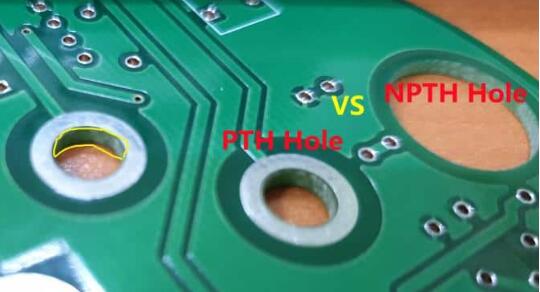
PTH refers to the pore, so the layer connected to it is conductive; There is an electrical connection. In contrast, NPTH non-metallic pores refer to the absence of copper on the inner side of the pores; Electrical partition.
PTH is a plated hole, which has two main uses in circuit boards. One is used for welding traditional DIP part feet. The diameter of this hole must be larger than the diameter of the part's welding foot so that the part can be inserted into the hole.

Another relatively small type of PTH, commonly known as via, is used to connect and turn off the copper conductor line between the double or double layers of circuit boards. As PCBs are composed of many copper conductor layers stacked and accumulated, each layer of copper conductor layer is covered with a cable sheath in the middle. In other words, the copper conductor layers cannot be connected, and their signal connection relies on via.
The main feature of PTH is that during the manufacturing process, after drilling, a thin copper layer is coated on the hole wall of the board to make it conductive. In this way, after the PCB assembly and manufacturing are completed, the connection resistance between the component leads and the copper wire is lower, and the mechanical stability is better. Now, most PCBs are double-sided or multi-layer, and most through-holes are plated. Components can be connected to the required layers in the circuit board. Plated through holes can also be plated with slots, plated with half holes (castle holes), not always in a circular shape.
Process flow of PTH
Decomposition of PTH process: alkaline degreasing → second or third stage countercurrent rinsing → coarsening (micro etching) → second stage countercurrent rinsing → pre leaching → activation → second stage countercurrent rinsing → degumming → second stage countercurrent rinsing → copper precipitation → second stage countercurrent rinsing → acid leaching
1. Alkaline degreasing: Remove oil stains, fingerprints, oxides, and dust in the holes on the board surface; Adjust the pore wall from negative charge to positive charge, facilitating the adsorption of colloidal palladium in subsequent processes; After oil removal, cleaning should be strictly carried out by the guidance requirements, and detection should be carried out using a copper deposition backlight test.
2. Micro etching: Remove oxides from the board surface, roughen the board surface, and ensure good adhesion between the subsequent copper deposition layer and the substrate copper; The newly formed copper surface has strong activity and can effectively adsorb colloidal palladium.
3. Pre-impregnation: Mainly used to protect the palladium tank from contamination by pre-treatment tank solution, extending the service life of the palladium tank. The main component is consistent with the palladium tank except for palladium chloride, which can effectively wet the pore wall and facilitate timely entry of subsequent activation solution into the hole for sufficient and effective activation.
4. Activation: After adjusting the polarity of alkaline oil removal through pre-treatment, the positively charged pore wall can effectively adsorb enough negatively charged colloidal palladium particles to ensure the average, continuity, and density of subsequent copper deposition; Therefore, oil removal and activation are crucial for the quality of subsequent copper deposition.
5. Gel release: Remove the tin ions wrapped around the colloidal palladium particles, expose the palladium nuclei in the colloidal particles, and directly and effectively catalyze the initiation of the chemical copper deposition reaction. Experience has shown that using fluoroboric acid as a gel release agent is a good choice.
6. Copper precipitation: Through the activation of palladium nuclei, a chemical copper precipitation self-catalytic reaction is induced. The newly formed chemical copper and reaction byproduct hydrogen can both serve as reaction catalysts to catalyze the reaction, allowing the copper precipitation reaction to continue continuously. After processing through this step, a layer of chemical copper can be deposited on the board or hole wall. During the process, the tank liquid should be stirred with normal air to convert more soluble divalent copper.
PTH is a major process in circuit board production, where copper deposition is called through-hole plating, also known as chemical copper plating. A thin layer of chemical copper is deposited chemically on a non-conductive hole wall substrate that has been drilled, to serve as the substrate for subsequent copper plating.