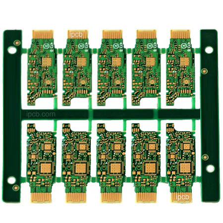
HDI is the abbreviation for High-Density Interconnector, which is a technology used to produce printed circuit boards. It is a circuit board that uses micro-blind buried hole technology and has a relatively high circuit distribution density. HDI is a compact product designed specifically for small-capacity users.

Application of HDI
Electronic design is constantly improving the overall performance of the machine while also striving to reduce its size. From smartphones to small portable products with smart weapons, 'small' is an eternal pursuit. HDI technology can make terminal product design more miniaturized while meeting higher standards of electronic performance and efficiency. HDI is widely used in mobile phones, digital cameras, MP3, MP4, laptops, automotive electronics, and other digital products, among which mobile phones are the most widely used. HDI boards are generally manufactured using the Build method, and the more times they are stacked, the higher the technical level of the board. Ordinary HDI boards are stacked once, while higher-order HDI uses two or more layers of technology, as well as advanced PCB technologies such as hole stacking, electroplating filling, and laser direct drilling. High-level HDI boards are mainly used for 3G mobile phones, advanced digital cameras, IC carrier boards, etc.
Processing Technology of HDI
HDI processing technology is a high-density circuit board processing technology with high technical requirements. However, the circuit boards produced have the characteristics of small size, light weight, and fast signal transmission rate, so they are widely used in various fields.
The main feature of HDI processing technology is to reduce the line width, line spacing, blind holes, stacked holes and other components to the micrometer level, and use high-tech processes to process surface mount products. The HDI processing process can be divided into the following steps:
1. Preparation of printed wiring
Signal transmission is achieved by printing the wire lines on a single or multi-layer circuit board onto the surface of the circuit board. This is usually achieved through photographic etching techniques, mechanical etching, or laser printing.
2. Blind hole preparation
Blind holes are a way of connecting different layers of a circuit board. By using a special drilling machine, tiny holes can be drilled into the circuit board to achieve the effect of connecting different layers.
3. Preparation of stacked holes
Stacked holes are holes where two or more holes are directly stacked together. The preparation of stacked holes requires special copper layer treatment to ensure that different stacked holes can be connected normally.
4. Welding technology
The components on the circuit board need to be fixed to the circuit board through welding technology. At present, the main welding techniques include through-hole welding, surface mount welding, and so on.
Characteristics of HDI board
1) Wiring density: HDI boards have higher wiring density compared to regular PCBs. By using blind and buried hole technologies, HDI boards can achieve more signal circuits in smaller sizes, providing higher wiring density and more complex circuit designs.
2) Multi-layer structure: HDI boards usually adopt a multi-layer structure, including more than 4 layers. The multi-layer structure provides more signal layers, power layers, and layers, supporting complex signal transmission and circuit connections.
3) Small size: Due to the advantages of high-density wiring and multi-layer structure, HDI boards can achieve smaller sizes compared to ordinary PCBs. This makes HDI boards more suitable for applications that require compact packaging and space limitations.
4) High-precision manufacturing: The manufacturing process of HDI boards requires higher precision process control and advanced manufacturing equipment. For example, advanced techniques such as laser drilling and light drawing are used to ensure accurate hole positions and detailed circuit patterns.
5) High-precision manufacturing: The manufacturing process of HDI boards requires higher precision process control and advanced manufacturing equipment. For example, advanced techniques such as laser drilling and light drawing are used to ensure accurate hole positions and detailed circuit patterns.
HDI technology can make terminal product design more miniaturized while meeting higher standards of electronic performance and efficiency. HDI is widely used in mobile phones, digital cameras, MP3, MP4, laptops, automotive electronics, and other digital products.