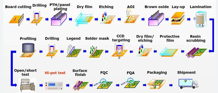
The steps for the fabrication of PCBs
1. Design circuit board layout
The design of a circuit board is the first step in the entire production process, which determines the shape, size, layout, and installation position of components of the circuit board. Designers use circuit design software for circuit board layout design, and layout according to circuit design requirements, including the position of components, routing paths, power and ground layout, etc.

2. Cutting: According to the PCB design requirements, use cutting tools to cut the insulation substrate into the required size circuit board.
3. Drilling: Use a CNC drilling machine for drilling operations, and drill holes on the circuit board according to design requirements, to install components and connect circuits.
4. Copper deposition: The process of depositing copper on a circuit board by uniformly depositing a copper layer on the board through chemical methods to increase conductivity and connectivity.
5. Film pressing: Place a protective film (usually a copper-coated film or cover layer) on the surface of the circuit board to protect the copper layer from corrosion and mechanical damage.
6. Exposure: Using lithography technology, transfer the designed circuit pattern to the surface of the circuit board. This usually involves placing the circuit board in a lithography machine and then exposing it through a light source and mask to form a circuit pattern with the photoresist.
7. Development: Place the exposed circuit board into the development solution, which will dissolve the unexposed photoresist and expose the copper layer.
8. Copper plating: Through electroplating technology, a thicker layer of copper is electroplated on the exposed and developed circuit board. This step can increase the conductivity and connectivity of the circuit board.
9. Tin plating: Immerse the circuit board in a solution containing tin to coat the copper surface with a layer of tin to protect the copper layer and provide a good soldering surface.
10. Stripping: Use appropriate chemical methods to remove the protective film and expose the areas on the circuit board that need to be soldered and assembled.
11. Etching: Place the circuit board into an etching solution to etch off unprotected copper. The etching solution will etch off unwanted copper layers, forming circuit patterns.
12. Tin removal: Use appropriate methods to remove unnecessary tin layers.
13. Optical testing: Use optical equipment, such as a microscope or automatic optical testing system, to check the patterns and connections on the circuit board. This step is used to ensure quality and correctness.
14. Solder resist oil: Apply a layer of solder resist oil on the circuit board to protect the circuit and mark the welding position. Solder blocking oil can prevent short circuits and contamination during the welding step, and provide better reliability and insulation performance.
15. Solder resist exposure and development: Place the circuit board coated with solder resist oil into the solder resist exposure machine, and use photolithography technology to transfer the designed solder resist pattern onto the circuit board. Then, place it in the developing solution, remove the unexposed solder mask, and form the desired solder mask pattern.
16. Characters: Print or engrave necessary characters, such as identifiers, serial numbers, etc., on the circuit board as needed. These characters are used to identify the circuit board and provide relevant information.
17. Surface treatment: Special treatment shall be applied to the surface of the circuit board as required. This may include anti-oxidation treatment, anti-corrosion treatment, or other surface coatings to improve the performance and durability of the circuit board.
18. Forming: Cut, bend, or otherwise shape the circuit board as needed to obtain the final desired shape and size.
19. Electrical testing: Conduct electrical testing on the circuit board to verify its connectivity and normal functionality. This can include using testing equipment and measuring tools to check parameters such as resistance, capacitance, and connectivity.
20. Final inspection: Conduct a comprehensive terminal inspection on the circuit board that has completed electrical testing. This includes visual inspection, dimensional measurement, identification inspection, etc., to ensure that the circuit board meets quality standards and regulatory requirements.
21. Sampling: Randomly select some circuit boards from batch production for sampling and testing to ensure the quality stability and consistency of the entire production batch.
22. Packaging: Properly package the circuit boards that have passed the final inspection to protect them from moisture, static electricity, and mechanical damage.
The fabrication of PCB is a very rigorous process, and every step requires strict adherence to the process flow. Excellent circuit board factory processes can ensure the quality of circuit boards, resulting in higher quality and more stable performance of electronic products.