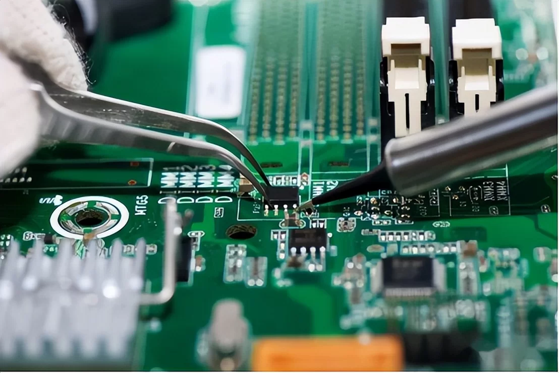
Patches PCB emerge as a crucial element, offering versatility, efficiency, and practical solutions to a myriad of electronic design challenges. In this comprehensive guide, we delve deep into the world of Patches PCB, exploring their significance, applications, design considerations, fabrication processes, and future prospects.
1. Understanding Patches PCB:
At its core, a PCB patch refers to a small, specialized circuit board designed to address specific electronic requirements within a larger system. These patches are often employed for various purposes, including signal conditioning, power distribution, voltage regulation, impedance matching, and fault correction, among others. Unlike conventional PCBs, which may encompass complex layouts and multiple layers, patches are typically compact and straightforward, tailored to fulfill precise functions within electronic devices.
2. Applications of Patches PCB:
The versatility of Patches PCB renders them indispensable across a wide spectrum of industries and applications. From consumer electronics to aerospace engineering, this find utility in:
Signal Enhancement: Amplifying weak signals or filtering out unwanted noise.
Power Management: Regulating voltage levels, distributing power, and protecting sensitive components.
Sensor Interfaces: Providing connectivity and processing capabilities for various sensors.
Embedded Systems: Serving as dedicated modules for microcontrollers, memory storage, or wireless communication.
Automotive Electronics: Facilitating diagnostics, control systems, and driver assistance features.
Medical Devices: Supporting diagnostic tools, monitoring equipment, and implantable devices.

Patches PCB
3. Design Considerations :
Creating effective PCB requires meticulous attention to design considerations to ensure optimal performance and compatibility. Key factors to consider include:
Form Factor: Determining the physical dimensions and shape of the patch to fit within space constraints.
Component Selection: Choosing components with suitable specifications and characteristics for the intended application.
Signal Integrity: Ensuring signal integrity by minimizing signal distortion, crosstalk, and electromagnetic interference.
Thermal Management: Implementing thermal relief measures to dissipate heat and prevent component overheating.
Reliability: Designing for robustness and durability to withstand environmental conditions, mechanical stress, and long-term operation.
Manufacturing Constraints: Adhering to manufacturing constraints such as assembly tolerances, material availability, and cost considerations.
4. Fabrication Processes for Patches PCB:
The fabrication of Patches PCB follows a systematic process involving several stages, including:
Design and Layout: Creating a schematic and PCB layout using specialized design software.
Material Selection: Choosing appropriate substrate materials, copper thickness, and surface finish based on application requirements.
Prototyping: Fabricating a prototype patch to validate the design and functionality before mass production.
Manufacturing: Using techniques such as etching, drilling, soldering, and surface mounting to fabricate the final Patches PCB.
Testing and Quality Assurance: Conducting thorough testing and inspection to verify functionality, reliability, and adherence to specifications.
5. Future Trends and Innovations:
As technology continues to evolve, so too will the field of Patches PCB, with several emerging trends and innovations shaping its trajectory:
Miniaturization: Advancements in miniaturization techniques will enable the development of smaller, more compact PCB for portable and wearable devices.
Integration: The integration of advanced functionalities, such as wireless connectivity, sensor fusion, and artificial intelligence, into Patches PCB will enhance their capabilities and versatility.
Flexible Substrates: The adoption of flexible substrates and printed electronics will enable the creation of flexible and conformal itfor curved surfaces and irregular geometries.
Sustainability: Increasing emphasis on sustainability and environmental responsibility will drive the development of eco-friendly materials and manufacturing processes for Patches PCB.
3D Printing: The utilization of additive manufacturing techniques, such as 3D printing, will revolutionize PCB patch fabrication, offering greater design freedom and faster prototyping capabilities.
Conclusion:
In conclusion, Patches PCBrepresent a pivotal component in the landscape of electronic design, offering tailored solutions to diverse challenges across various industries. By understanding their significance, applications, design considerations, fabrication processes, and future trends, engineers and innovators can harness the full potential of it drive technological advancement and innovation in the digital age.
Through continuous research, innovation, and collaboration, the realm of this PCB will continue to evolve, pushing the boundaries of what is possible and shaping the future of electronics in profound and transformative ways. As we embark on this journey of discovery and innovation, the possibilities are limitless, and the future is bright for PCB and the world of electronic design as a whole.