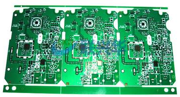
As surface array packaging is becoming more and more important, especially in the fields of automotive, telecommunications and computer applications, productivity has become the focus of discussion. The pin pitch is less than 0.4mm, which is 0.5mm. The main problem of fine pitch QFP and TSOP packages is low productivity. However, because the pitch of the surface array package is not very small (for example, the flip chip is less than 200μm), after reflow, the dmp rate is at least 10 times better than the traditional fine-pitch technology. Furthermore, compared with QFP and TSOP packages with the same pitch, considering the automatic alignment during reflow soldering, the requirements for smt placement accuracy are much lower.
Another advantage, especially for flip chip, the footprint of the printed circuit board is greatly reduced. The surface array package can also provide better circuit performance. Next, the editor will continue to explain and analyze the content in the article "Fast smt placement of advanced packaging devices".
1. Placement accuracy

In order to have an overall understanding of different placement equipment, you need to know the main factors that affect the placement accuracy of the area array package. The ball grid placement accuracy P//ACC// depends on the type of ball grid alloy, the number of ball grids and the weight of the package.
These three factors are interrelated. Compared with ICs in QFP and SOP packages with the same pitch, most surface array packages have lower mounting accuracy requirements.
For round pads without solder mask, the maximum allowable mounting deviation is equal to the radius of the pad. When the mounting error exceeds the radius of the pad, there will still be mechanical contact between the ball grid and the pad. Assuming that the diameter of the usual pad is roughly equal to the diameter of the ball grid, the placement accuracy of the μBGA and CSP packages with a ball grid diameter of 0.3mm and a pitch of 0.5mm is required to be 0.15mm; if the ball grid diameter is 100μm and the pitch is 175μm, The accuracy requirement is 50μm.
In the case of tape ball grid array packages (TBGA) and heavy ceramic ball grid array packages (CBGA), self-alignment is limited if it occurs. Therefore, the precision requirements for placement are high.
2. Application of flux
The furnace used for standard large-scale reflow soldering of flip chip ball grids requires flux. Nowadays, the more powerful general-purpose SMD placement equipment has built-in flux application devices, and the two commonly used built-in supply methods are coating and dip soldering.
The coating unit is installed near the placement head. Before flip chip placement, apply flux to the placement position. The dose applied in the center of the mounting position depends on the size of the flip chip and the wetting characteristics of the solder on the specific material. It should be ensured that the flux coating area is large enough to avoid missing pads due to errors.
In order to perform effective filling in a non-cleaning process, the flux must be a non-cleaning (no residue) material. Liquid flux always contains very little solid matter, and it is most suitable for non-cleaning processes.
However, due to the fluidity of the liquid flux, after flip chip placement, the movement of the placement system conveyor belt will cause the inertial displacement of the chip. There are two ways to solve this problem:
Set a waiting time of several seconds before the board is sent. During this time, the flux around the flip chip evaporates quickly to improve the adhesion, but this will reduce the yield.
SMT patch proofing manufacturers can adjust the acceleration and deceleration of the conveyor belt to match the adhesion of the flux. The smooth movement of the conveyor belt will not cause wafer displacement.
The main disadvantage of the flux coating method is that its cycle is relatively long. For each device to be coated, the mounting time increases by about 1.5s.
3. Dip soldering method
In this case, the flux carrier is a rotating bucket, and a blade is used to scrape it into a flux film (about 50μm). This method is suitable for high-viscosity flux. By only dipping the solder on the bottom of the ball grid, the consumption of solder can be reduced during the manufacturing process.
This method can use the following two process sequences:
1) Mounting is performed after the optical ball grid is aligned and the ball grid is dipped in solder. In this sequence, the mechanical contact between the flip chip ball grid and the solder carrier will negatively affect the placement accuracy.
2) After the ball grid dipping flux and the optical ball grid are aligned, mount it. In this case, the flux material will affect the alignment image of the optical ball grid.
The dipping flux method is not very suitable for the flux with high volatilization ability, but its speed is much faster than the coating method. Depending on the mounting method, the additional time for each device is approximately 0.8s for pure picking and mounting, and 0.3s for collecting and mounting.
When using standard SMT to mount μBGA or CSP with a ball grid pitch of 0.5mm, there are still some things that should be noted: For products using hybrid technology (standard SMD using μBGA/CSP), the most critical process is obviously flux Coating printing. Logically, it is also possible to use a mounting method that integrates the traditional flip-chip process and the application of flux.
All surface array packages have shown potential in performance, packaging density and cost savings. In order to give full play to the effectiveness of the overall field of electronic production, further research and development are required, and the manufacturing process, materials and equipment need to be improved. As far as SMD placement design equipment is concerned, a lot of work is focused on vision technology, higher output and precision.