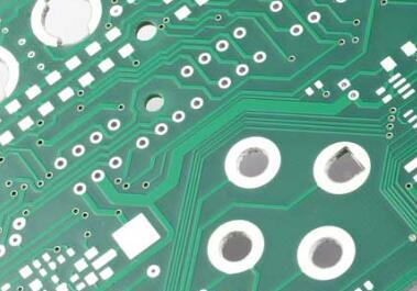
PCB blind vias are conductive holes that connect the surface and inner layers without penetrating the entire board. Blind vias are located on the top and bottom surfaces of printed circuit boards, with a certain depth, used for connecting the surface circuit and the inner circuit below. The depth of the holes usually does not exceed a certain ratio (aperture).

Blind via are common in high-density interconnect (HDI) PCBs. The increased complexity of blind vias enables designers to improve Signal integrity while reducing PCB size. The use of blind through-holes provides a series of new routing options and choices, as precious space is no longer needed for through-holes, which pass through unconnected layers.
Blind vias reduce parasitic capacitance by reducing the length and width of the vias. When a signal passes through a through-hole, signal attenuation and reflection occur. In high-speed design, signal discontinuity (capacitive and/or inductive discontinuity) generated by through-holes can affect the integrity of the signal and power. Blind vias are a good way to connect high-speed (above 5gb/s) signal lines.
The Process of Manufacturing PCB Blind-via
1. Sequential lamination
In this process, an extremely thin laminate undergoes all the production steps required to manufacture a double-sided PCB. It is drilling, etching, and plating. Subsequently, this layer is stacked with all other layers of the PCB. The number of manufacturing steps involved in this method of manufacturing blind vias makes it very expensive.
2. Photo defined
This manufacturing process involves laminating photosensitive resin sheets onto the core. The pattern covering the photosensitive film is exposed to light, making the remaining material hard. Remove the material from the hole using an etching solution. Copper is plated on the holes and outer surface to create the outer layer of the PCB. When there are a large number of blind vias on the PCB, this blind via production method is cost-effective.
3. Controlled depth
This method uses the same drilling process as through-hole drilling. In addition to drilling a certain depth hole on the PCB and then plating it on. Generally speaking, drilling is a cost driver, but this method is the cheapest way to manufacture blind via, but the minimum width that can be drilled depends on the smallest available drill bit size, typically 0.15 mm.
4. Laser drilled
This process is completed after all layers of the PCB are laminated, but before the outer layer is etched and laminated. By laser drilling copper and dielectric materials in one stage, a through hole can be created. This is an economically effective method. To reduce costs and shorten production time, laser drilling holes may be a better choice than through holes.
The Function of PCB Blind via
1) Reduce signal interference
In PCB circuit boards, the transmission of signals is subject to many interferences, which may lead to signal distortion and transmission errors, thereby affecting the performance and stability of electronic products. Blind via PCB circuit boards can reduce noise interference in PCB circuit boards, optimize signal transmission paths, ensure signal transmission speed and stability, and improve the overall performance of electronic products.
2) Increase board density and number of holes
With the development of electronic products, the density of modern circuit boards is increasing, and the number of holes is also increasing. Blind buried hole PCB circuit boards can increase the number of holes and make them more compact without occupying the surface of the circuit board, resulting in a higher density of the PCB circuit board. The structure of blind-via PCB circuit boards enables them to carry more electronic components within the same PCB area range, improving the functionality and performance of electronic products.
3) Improving the stability of electronic products
The stability of electronic products is an important indicator for evaluating the quality of a product. The layout of holes and signal paths in blind hole PCB circuit boards is very standardized, which can stably receive and transmit signals, effectively reduce product failure rates, and improve the stability and reliability of electronic products.
PCB blind via circuit boards plays a crucial role in the performance and stability of electronic products. They can reduce signal interference, increase board density and number of holes, and improve the stability of electronic products.