In this article, we will discuss proximity effects and discuss how to apply knowledge about proximity effects and skin effects to circuit board wiring and signal paths to minimize the impact of noise on the system. At the same time, we will also discuss other types of noise sources and methods to reduce these noises in order to ultimately minimize the noise in the circuit.
Proximity effect
Proximity effect refers to the interaction of two adjacent conductors whose current flows in opposite directions, so that the current tends to be concentrated in the adjacent areas, as shown in Figure 1.
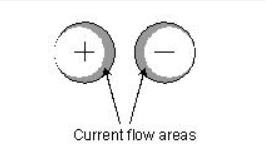
Figure 1. The proximity effect makes currents flowing in opposite high-frequency currents always keep as close as possible
Due to the skin effect, the AC current is mainly concentrated on the surface of the conductor.
When the distance between two conductors is close, and/or the signal frequency increases, the proximity effect will make the currents flowing through two adjacent conductors closer together. The reason for the proximity effect is that the current always looks for the path with the least impedance. Among other elements, the path with the least impedance generally refers to the path that minimizes the strength of the magnetic field surrounding the conductor.
The DC return current fills the entire conductor, while AC does not. The so-called path with the least impedance is the part where the magnetic fields generated by the two conductors with opposite current directions are closely combined with each other. This is also the reason why the currents of the two conductors with opposite current directions are close to each other. This makes the diversion line of the return plane attracted by its corresponding reverse flow line below, making them close to each other, as if the return plane is a path that conducts the return signal immediately below the outflow path, as shown in Figure 2.
Please note that here we are talking about the return plane, not the ground plane. The reason for this is that the return signal is sometimes conducted through the ground plane and sometimes through the power plane. Regardless of the plane, as long as the return signal is conducted, it is called the return plane.
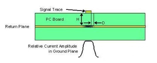
Figure 2. The proximity effect makes the two relatively high-frequency current conducting wires as close to each other as possible
The current density (IRP) of the return plane decreases rapidly as the distance from the edge of the outgoing signal path increases, as shown in Equation 1.

Where:
IRP represents the current density at the horizontal distance "D" from the path carrying the outgoing signal on the reference plane
i represents the signal current
H represents the distance between the path carrying the outgoing signal and the reference plane
D represents the horizontal distance from the path carrying the outgoing signal
The current of the return plane closely follows the path carrying the outgoing signal above (or below) it. When the D/H ratio is 5, the current density "D" from the edge of the path carrying the outgoing signal will drop below 4%; when the D/H ratio is 10, the current density from the edge of the path carrying the outgoing signal The current density at "D" will drop below 1% directly below it. As a result, the alternating current of the return plane is basically limited to the area below the path carrying the corresponding outgoing signal. This is why we do not need to divide the ground plane when considering PCB layout. Moreover, the division of the ground plane can cause serious radiation problems. Although many designers try to solve this problem with costly shielding, they are in vain.
The return current of the reference plane closely follows its corresponding outgoing current. Therefore, as long as the paths of the outgoing current are kept at a sufficient distance, the mixing of the return plane currents can be avoided. It is the mixing of the return plane currents that produces Crosstalk and noise. The distance between the lines mentioned here is a function of the distance between layers (the "H" in Figure 2 and Equation 1).
According to the current density formula, the current density relative to any point (or distance "D") from the edge of the path carrying the outgoing signal can be calculated. Please note that this formula calculates current density, not current.
The typical distance "H" depends on the path carrying the outgoing signal and the actual position of the return plane on the printed circuit board:
If it is between the outer layer and the inner layer, the typical "H" value of the 4-layer and 6-layer circuit boards are both 75 mill;
If it is between two inner layers, the typical "H" value for a 4-layer circuit board is 39 mill, and the typical "H" value for a 6-layer circuit board is 14 mill.
Please consult the circuit board supplier for the spacing between the planes of the circuit board you are using.
If the distance between the edges of the path reaches 4 times the distance between the paths carrying the outgoing signal and the return signal, the crosstalk will drop to less than 6% of the signal amplitude.
The combined influence of proximity effect and skin effect
As a result of the combination of the proximity effect and the skin effect, the current-carrying area of the conductor occupies only a small part of its entire cross-section, and the actual current-carrying area is much smaller than that shown in Figure 3.
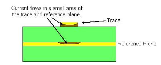
Figure 3: The combined effect of the skin effect and the proximity effect is that the area where the conductor actually carries current is greatly reduced
Both the skin effect and the proximity effect cause the current-carrying area of the conductor to be smaller than the cross-section of the conductor, so they both increase the AC resistance of the conductor.
The influence of PCB layout on its performance
In addition to the skin effect and proximity effect, high-frequency circui ts have another problem that is manifested as electromagnetic interference (EMI). This problem is manifested in two aspects: signal radiation and signal reception.
Today's governments all have specific regulations on the radiation energy allowed by the equipment. Limiting the radiated energy of the device can reduce the interference signal received by the circuit. In a sense, these regulations are very good. At the same time, we need to take measures to ensure that our circuits cannot radiate unauthorized frequency interference signals. Design practice also tells us that proper measures must be taken during the circuit design process to prevent the circuit from receiving surrounding interference signals. In any case, we cannot be sure when the circuit will be exposed to an environment with strong interference.
When the outflow current and the return current flow, the area between the outflow path and the return path is called the "circular area". The larger the circulation area, the larger the electromagnetic field surrounding the conductor. The radiation is generated by the surrounding electromagnetic field. The larger the circulation area, the greater the energy received by electromagnetic radiation or electromagnetic coupling. Since high-frequency current flows along a very narrow path on the return plane, the path is like a path and emits radiation, especially when the return current path on the ground plane is forced to deviate due to the ground plane being divided. The radiation is more serious when carrying the path corresponding to the outgoing current. Therefore, dividing the ground plane is by no means a good method.
People usually fill unused areas on the printed circuit board with a grounded copper film. However, if the copper film used for filling is only grounded through one point, it is actually equivalent to designing a ground plane that can flow through that point. An antenna that radiates energy. Therefore, if you cannot ground through more than one point, you should avoid using this copper film filling mode.
Another common method is to use a single ground plane and power circuit path. The problem with this method is that the equivalent series inductance (ESL) of the capacitor will cause the impedance of the capacitor to change with frequency, as shown in Figure 4. Using multiple capacitors with different tolerances can expand the frequency range that is effectively bypassed, but when the frequency exceeds a few hundred MHz, the capacitor is no longer useful. If the designer thinks that there is no such high-frequency signal in the circuit, we may wish to consider the fact that the square wave contains harmonic components exceeding the 30th harmonic. The frequency of the 30th harmonic of a 40 MHz digital signal is 1.2 GHz (1,200 MHz).
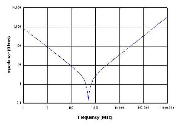
Figure 4: Capacitors can bypass the signal in a very narrow frequency range
The most effective way to bypass these high-frequency components is to use interlayer capacitance between the power plane and the ground plane, and the capacitance formed between the power plane and the ground plane for the path for transmitting power is too small to produce Sufficient high-frequency bypass function.
As we all know, if the edge effect is ignored, the interlayer capacitance is:
C = k o A / d
Among them, k = the relative permittivity of the interlayer dielectric
o=8.854 x 10⁻¹² farads/meter
A=the area of the two plates of the capacitor
d = the distance between the two plates of the capacitor
If we assume an FR-4 circuit board with k=4.1 and the distance between the two inner layers is 39 mills, then calculated according to Equation 2, the interlayer capacitance is about 3.67pf/cm2, or 23.65pf/inch2.
Circuit considerations
Earlier we discussed some important wiring issues that need to be considered when designing mixed-signal circuit devices (such as ADCs and DACs), but for noise processing, this is far from enough. Next we discuss how the input and output circuits generate noise and how to prevent these problems.
Input drive considerations
Most ADCs produced today can be regarded as sampling converters, that is, they sample the input signal and convert the sampled voltage into a corresponding value. Figure 5 shows a simplified equivalent circuit for sampling the ADC input signal. In the figure, "CIN" represents the input capacitance of the pin, "CS" represents the sampling capacitor, "S" represents the sampling switch, and "RON" represents the switch at Resistance in the on state. When sampling, the switch "S" is closed, and the sampling capacitor "CS" is charged to the input voltage level; in the conversion gap when the switch "S" is open and another switch (not shown in the figure) is closed, according to the different ADC design, The voltage applied on the sampling capacitor is transferred to another capacitor or capacitors.
When the switch is closed again for the next sampling, since the voltage on the sampling capacitor is transferred elsewhere, the voltage on the sampling capacitor is different from when the switch was opened last time. In order to charge the sampling capacitor again, a current pulse is generated at the input of the ADC, and the current pulse causes a voltage spike at the input of the ADC. Unless the sampling capacitor fails to charge to a sufficiently effective signal level before the switch is turned off again, generally speaking, such voltage spikes at the input will not cause any problems. The important thing is that the sampling input signal must be turned off again after the switch is turned off. The effective signal level was reached before.
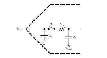
Figure 5: Most ADCs use sample inputs
The capacitor at the input of the ADC circuit can accumulate charge to alleviate the current demand on the drive source, so that it can quickly stabilize. However, generally speaking, the output of the operational amplifier cannot "tolerate" a larger capacitance, so we usually use the amplifier A resistor in series at the output isolates it from the capacitor, as shown in Figure 6.
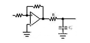
Figure 6: Most ADCs use sample inputs
So, how to determine the value of the resistance Rf and the capacitance Cf in Figure 6? An effective method is to first take 10 times the capacitance limit of the sampling capacitor CS as the value of Cf, and then calculate the value of Rf according to Equation 3, where "n" is the resolution (number of bits) of the ADC.
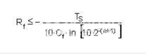
Output capacitance considerations
The inductance of the bonding wire isolates the well-bypassed output wire from the silicon chip. When the ADC output pin signal changes from low to high, we can observe the negative pulse on the output line, which we call "power bounce". If this output line is used as an output stage and is also shared by other areas on the same silicon chip, these negative pulses will be added to the signals in these areas. If the area is a digital circuit, these negative pulse waves will cause jitter noise; if it is an analog circuit, these negative pulse waves will directly introduce noise into the conversion process.
When the digital output changes from high to low, the charge accumulated on the bus capacitance and the input capacitance of the driven device will flow through the surface of the silicon chip and the ground pin of the ADC. The ground coupling inductance isolates the DC output of the silicon chip from the stable, noise-free ground and impulse pulses of the device pins. The amplitude of these pulses will vary with the number of discharged output terminals. This phenomenon is called "ground bounce." The DC component voltage of the silicon chip is neither consistent with the ground wire, nor a stable voltage, but fluctuates, making noise between the input signal and the ground wire due to the voltage difference, and this noise is converted again, such as Shown in Figure 7.
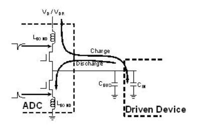
Figure 7: The current required to charge and discharge the output capacitor will generate noise in the silicon chip
For ADCs with differential inputs, you may think that the common mode rejection (CMR) of the differential inputs can solve the above-mentioned problems. In fact, the CMR of any circuit will gradually fail with the increase of the noise frequency, especially when the signal frequency exceeds several hundred KHZ, the effect of CMR is even worse. Since the frequency of these ground bounce pulses is usually close to the frequency of the output data, and the fast voltage rise time corresponds to a higher frequency, the effect of CMR is almost zero for the above-mentioned high-frequency signal range.
Therefore, our task is to minimize these charging and discharging currents in order to minimize the induced noise.
The first step to reduce this type of induced noise is to reduce the capacitive load on the digital output pins, which means that it should be avoided to directly drive the bus directly with the ADC output (this is why the high-speed ADC still uses the traditional three-state output mode Reason). A smaller capacitance means that the amount of charge that needs to be moved during charging is reduced, so the induced noise generated is naturally lower. Therefore, a very important point in the design is to try to make the device being driven have a single, low-capacitance input pin, and the input end of the device should be as close as possible to the output pin of the ADC.
However, in some cases, it is impossible to reduce the output capacitance to a level sufficient to eliminate the induced noise caused. This is especially true when the accuracy of the ADC is high, the reference voltage and signal voltage levels are low, and the sampling rate is high. At this time, it is helpful to connect a 47-100 ohm resistor in series as close as possible to the ADC output pin, because the series resistor can limit the current of the ADC output pin capacitor charging and discharging, and reduce the noise on the chip. See Figure 8.
If the series resistor is not placed as close as possible to the ADC digital output pin, the board-to-board capacitance between the ADC and the series resistor will increase, and thus generate higher noise than the original noise. Similarly, with the improvement of the accuracy of the analog-to-digital conversion device, the reduction of the reference voltage and signal voltage level, and the improvement of the sampling rate, the situation is even more so. Of course, we must try to shorten the total length of these digital transmission lines.
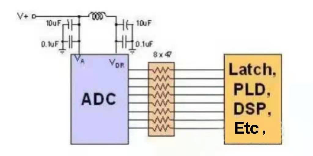
Figure 8: The series resistance at the ADC output can reduce the noise caused by the charging and discharging of the output capacitor
Comprehensive elaboration
All signal-carrying lines are transmission lines. When the length of the line exceeds a certain threshold, the line must be treated as a transmission line to avoid signal distortion, timing deviation, jitter, and noise.
As the signal frequency increases, the skin effect and proximity effect will increase the actual component (resistance) of the line impedance. When other lines are close to or far away from the transmission line, the impedance of the transmission line will change accordingly, resulting in uneven impedance distribution across the transmission line. Therefore, how to deal with the transmission line is extremely important in wiring. The same is true for the return path of the return plane. Interlayer capacitances are extremely important because they can bypass high-frequency signal components that are not eliminated by scattered capacitors.
In general, a reasonable design of the ADC driving circuit and reducing the output current will help reduce the noise that will damage the internal performance of the circuit.