(1) When drawing schematic diagram, the annotation of pin must use network NET rather than TEXT, otherwise there will be problems when guiding PCB
(2) when drawing the schematic diagram, we must make all the components have packaging, otherwise when guiding the PCB, we will not find the components. Some components can not be found in the library, so we should draw by ourselves. In fact, we should draw by ourselves. To RENAME a COMPONENT, start FILE/NEW -- select SCH LIB -- to enter the Parts editing library. The component package is drawn the same way, but in PCB LIB, the component border is in the TOPOverlay layer, which is yellow.

(3) To rename the elements in order, select TOOLS ---- and ANNOTATE the ANNOTATE annotation and select the order
(4) Before conversion into PCB, to generate reports, mainly network table select DESIGN DESIGN ---- "Creat Netlist to create network table
(5) There is to check the rules of electrical appliances to choose TOOLS. ERC
(6) Then PCB can be generated. If there is any error in the process of generation, the schematic diagram must be modified correctly and recycled into PCB
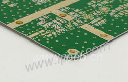
(7) PCB must first step well, should make the line as short as possible, as few holes as possible.
tools -- Design Rules, Routing (Constrain) GAP 10 or 12, Routing VIA STYLE set hole, maximum and minimum external diameter of han plate, Maximum inner diameter, the size of minimum inner diameter. Width Constraint sets the line Width, Max and min
(9) the width of the line drawing general common of the 12 mil, peripheral circuit power supply and ground wire is 120 or 100, the power of the film and the land was 30 or 40 or 50, to coarse crystal town line, should be placed by single chip microcomputer, common line is thick, long line to coarse, line can't turn right Angle to 45 degrees, the power supply and there are other signs must be marked in the TOPLAY, Convenient debugging cable. If you find that the diagram is not correct, you must first change the schematic diagram, and then use the schematic diagram to replace the PCB.
(10) The bottom option in the VIEW option can be either Inch or millimeter