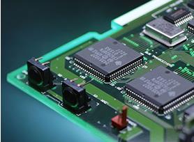
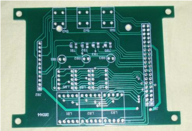
Considering the signal quality control factors, the general principles of PCB board cascade design are as follows:
1. The second layer adjacent to the component surface is the ground plane, which provides the shielding layer of the device and the reference plane for the top-level wiring.
2. All signal layers are adjacent to the ground plane as far as possible to ensure a complete backflow channel.
3. Try to avoid direct adjacency between two signal layers to reduce crosstalk.
4. the main power supply as far as possible corresponding to adjacent, form a plane capacitance, reduce the plane impedance of the power supply.
5. take into account the laminated structure symmetry, conducive to plate production warpage control.

The above is the general principle of cascade design, in the actual development of cascade design, circuit board designers can increase
the distance between adjacent wiring layer, reduce the distance between the corresponding wiring layer and the reference plane, and then control the cross-talk rate of wiring between layers, can use two signal layers directly adjacent. For the consumer products that pay more attention to cost, the way of reducing plane impedance by adjacent power supply and ground plane can be weakened, so as to reduce wiring layer as much as possible and reduce PCB cost. This, of course, comes at the cost of signal-quality design risk.
For the layered design of Backplane (or midplane), it is difficult for common backplanes to make adjacent cables perpendicular to each other, which inevitably leads to parallel long-distance cabling. For high-speed backplanes, the general cascading principle is as follows:
1. The Top and Bottom surfaces are complete ground planes, which constitute the shielded cavity.
2, no adjacent layer parallel wiring, to reduce crosstalk, or adjacent wiring layer spacing is far greater than the reference plane spacing.
3. All signal layers are adjacent to the ground plane as far as possible to ensure a complete backflow channel.
It should be noted that the above principles should be flexibly mastered and applied in the specific PCB stacking setup. Reasonable analysis should be made according to the actual needs of the board to determine the appropriate stacking scheme.