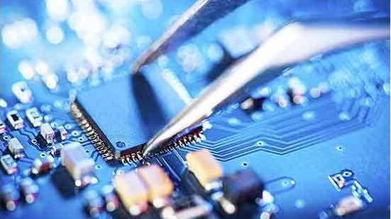
In daily life and work, it is often necessary to use a variety of electronic equipment and mechanical equipment. They have long been inseparable from daily life, and they have become necessities of daily life. Such as computers, mobile phones, etc. And the key component of those devices is PCB. PCB is also the circuit board, and the processing of the circuit board is changed to PCBA. Before the production and processing of PCB, PCBA design and processing must be carried out. So, what are the main methods of PCBA proofing?
1. Subtraction method. This kind of method mainly uses chemicals to remove the unnecessary places on the blank circuit board, and the remaining places are the necessary circuits. PCBA design and processing mainly use screen printing or photosensitive plates and engraving for processing. Remove unnecessary parts.
2. Additive method. This kind of method is to expose the necessary places through the combination of ultraviolet light and photoresist, and then use electroplating to thicken the certificate line, and then cover with an anti-etching resist or metal thin tin, and finally the photoresist and the copper under the cover The foil layer is etched away.

3. Multilayer method. This type of method is the most common method for PCB design and processing, and it is also the main method for making multilayer printed circuit boards. It is through the process from the inner layer to the outer layer, and then using the subtractive or additive method to process, the process of repeating the layering method continuously, so as to realize the production of multi-layer printed circuit boards. The most critical process is the build-up method, in which printed circuit boards are added layer by layer and repeated processing is performed.
The PCBA proofing refers to the whole process of the empty PCB board passing through smt and then passing through the DIP plug-in, which is called PCBA proofing. It is the behavior of the customer to perform the smt patch test again because of the need of the new product. Nowadays, PCBA processing technology is widely used in life, and the fields involved are mainly concentrated in the field of science and technology.
Although PCBA processing technology is widely used in daily life, many people do not know what the documents should be prepared when doing this work. After research, it is found that the documents that need to be prepared for PCBA proofing mainly include the following:
First of all, we must prepare a complete and accurate BOM. Then provide a template Gerber file. Provide as much as possible the product number silk screen image and patch coordinate file, and finally need to provide the PCB file.
In addition to the above-mentioned documents that need to be prepared, there are some precautions that have to be mentioned when proofing. Because these precautions will make the whole work more efficient and make the quality of the products more high-quality. In the process of PCBA processing technology, you need to pay attention to the following points:
First of all, when preparing materials for the outbound SMT processing capacity, in order to use excess ingredients in the production process, several single and double panels should be prepared. Other low-value preparations should also be prepared. However, large originals and chips can be prepared without much preparation.