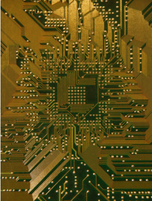
PCB board immersion gold process introduction
The gold immersion process is to generate a layer of plating through a chemical oxidation-reduction reaction method, which is generally thicker, which is a kind of chemical nickel-gold layer deposition method, which can achieve a thicker gold layer, which is golden yellow and has a better color. And generally softer.

PCB board spray tin process introduction
The tin spraying process, also called hot air leveling technology, is one of the most common surface coating forms for board surface treatment, which is to spray a layer of tin on the pads to enhance the conduction performance and solderability of the PCB pads .
The difference between Immersion Gold and Spray Tin:
1. The solderability of spraying tin is better than that of immersion gold, because there is already tin on the pad, it is easier to solder on the tin, and for general manual soldering, it is also very easy to solder.
2. The immersion gold board only has nickel and gold on the pads, and the solder mask on the circuit is more firmly combined with the copper layer. The signal transmission in the skin effect is on the copper layer, which generally does not affect the signal.
3. Most of the immersion gold will not have the phenomenon of black pads after assembly, so the immersion gold plate has a longer standby life, compared with the lower spray tin plate, which has a shorter standby life.
4. Immersion gold has better flatness, and it is difficult for the tin spray process to flatten the thin pads, which will bring difficulty to the placement of SMT.
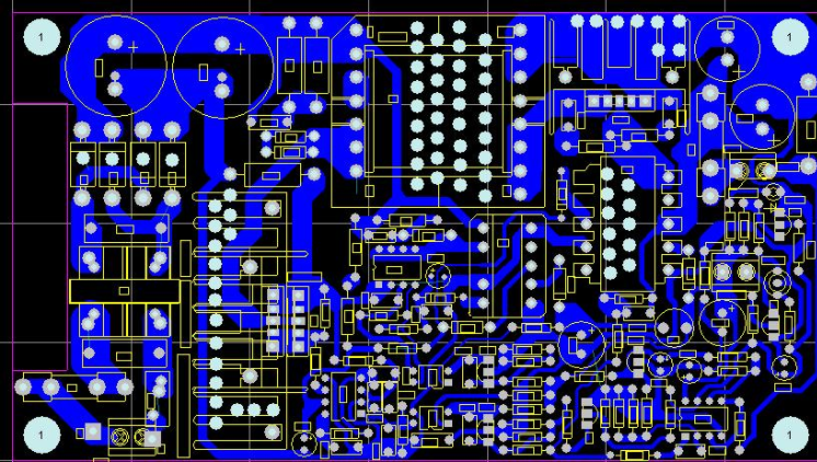
PCB board BGA introduction
The full name of BGA is Ball Grid Array (PCB with ball grid array structure), which is a packaging method in which integrated circuits use organic carrier boards. it has:

1. The package area is reduced.
2. The function is increased, and the number of pins is increased.
3. PCB board can be self-centered when welding, easy to tin.
4. High reliability.
5. Good electrical performance and low overall cost.
PCB boards with BGA generally have many small holes. Most customers' BGA vias are designed with a finished hole diameter of 8-12mil. The distance between the surface of the BGA and the hole is 31.5mil as an example, generally not less than 10.5mil. BGA via holes need to be plugged, BGA pads are not allowed to be filled with ink, and BGA pads are not drilled.
BGA pad design rules
1. The diameter of the pad can affect both the reliability of the solder joint and the wiring of the component. The diameter of the pad is usually smaller than the diameter of the solder ball. In order to obtain reliable adhesion, it is generally reduced by 20%-25%. The larger the pad, the smaller the wiring space between the two pads. For example, the 1.27mm pitch BGA package uses 0.63mm diameter pads, and two wires can be arranged between the pads, with a line width of 125 microns. If a pad diameter of 0.8 mm is used, only one wire with a line width of 125 microns can be passed.
2. the following formula gives the calculation of the number of wiring between two pads, where P is the package pitch, D is the diameter of the pad, n is the number of wiring, and x is the line width. P-D≥(2n+1)x
3. The general rule is that the diameter of the pad on the PBGA substrate is the same as that on the PCB.
4. CBGA pad design should ensure that the opening of the template makes the solder paste leakage ≥0.08mm. This is the minimum requirement to ensure the reliability of the solder joints.