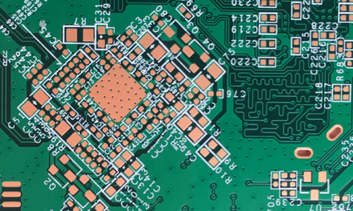
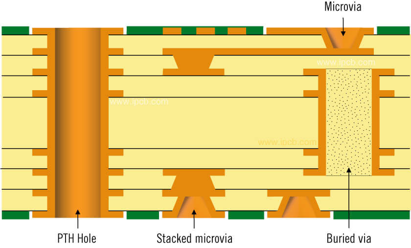
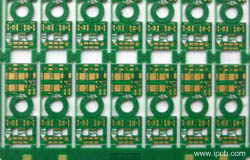
Circuits of different nature on the PCB circuit board must be separated, but they must be connected under the best conditions without electromagnetic interference. At this time, circuit board manufacturers need to use microvias. Generally, the diameter of micro vias is 0.05mm to 0.20mm. These vias are generally divided into three categories, namely blind vias, bury vias and through vias.
Blind holes are located on the top and bottom surfaces of the printed circuit board and have a certain depth. They are used to connect the surface line and the underlying inner line. The depth of the hole usually does not exceed a certain ratio (aperture). Buried hole refers to the connection hole located in the inner layer of the printed circuit board, which does not extend to the surface of the circuit board. The above two types of holes are located in the inner layer of the circuit board, and are completed by a through-hole forming process before lamination, and several inner layers may be overlapped during the formation of the via. The third type is called a through hole, which penetrates the entire circuit board and can be used for internal interconnection or as an adhesive positioning hole for components.

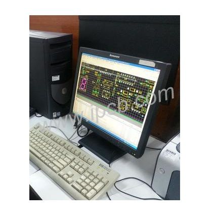
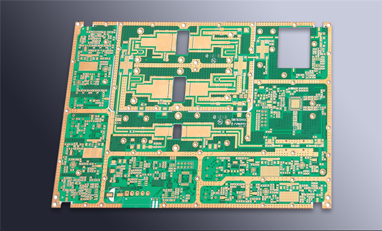
How to deal with the best high-speed PCB micro vias
When designing the RF circuit board, the high-power RF amplifier (HPA) and the low-noise amplifier (LNA) should be separated as much as possible. Simply put, keep the high-power RF transmitter circuit away from the low-noise receiver circuit. If there is a lot of space on the PCB, this can be done easily. But usually when there are many components, the PCB space becomes very small, so this is difficult to achieve. You can put them on both sides of the PCB board, or let them work alternately instead of working at the same time. High-power circuits sometimes include RF buffers and voltage-controlled oscillators (VCO).
Design partition can be divided into physical partition (physical partiTIoning) and electrical partition (Electrical parTITIoning). Physical partitioning mainly involves issues such as component layout, orientation, and shielding; electrical partitioning can continue to be divided into power distribution, RF wiring, sensitive circuits and signals, and grounding partitions.
Component layout is the key to achieving an excellent RF design. The most effective technique is to first fix the components on the RF path and adjust their position to minimize the length of the RF path. And keep the RF input far away from the RF output, and as far away as possible from high-power circuits and low-noise circuits.
The most effective circuit board stacking method is to arrange the main ground on the second layer below the surface, and route the RF lines on the surface as much as possible. Minimizing the size of the vias on the RF path can not only reduce the path inductance, but also reduce the virtual solder joints on the main ground and reduce the chance of RF energy leaking to other areas of the laminate.
In physical space, linear circuits like multi-stage amplifiers are usually sufficient to isolate multiple RF zones from each other, but duplexers, mixers, and intermediate frequency amplifiers always have multiple RF/IF signals that interfere with each other. Therefore, care must be taken to minimize this effect. The RF and IF traces should be crossed as much as possible, and a grounding area should be placed between them as much as possible. The correct RF path is very important to the performance of the entire PCB board, which is why the component layout usually takes up most of the time in the mobile phone PCB design.
On the mobile phone PCB board, usually the low noise amplifier circuit can be placed on one side of the PCB board, and the high power amplifier on the other side, and finally they are connected to one end of the RF antenna on the same side by a duplexer And the other end of the baseband processor. This requires some tricks to ensure that RF energy does not pass through the vias from one side of the board to the other. A common technique is to use blind holes on both sides. The adverse effects of vias can be minimized by arranging blind holes in areas where both sides of the PCB board are not subject to RF interference.