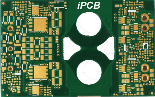
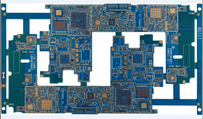
Before the PCB design of a multilayer PCB board, the PCB designer needs to determine the circuit board structure used according to the circuit scale, circuit board size and electromagnetic compatibility (EMC) requirements. After determining the number of PCB board layers, determine the placement of the inner electrical layer. And how to distribute different signals on these layers, this is the choice of multilayer PCB laminate structure. The laminate structure is an important factor that affects the EMC performance of the PCB board, and it is also an important means to suppress electromagnetic interference. Let’s learn about the lower laminate. Design Points.

1. The PCB stacking method is recommended to be the Foil stacking method
2. Minimize the use of PP sheets and CORE models and types in the same stack (each layer of medium does not exceed 3 PP stacks)
3. The thickness of the PP medium between the two layers should not exceed 21MIL (thick PP medium is difficult to process, generally adding a core board will increase the actual number of PCB stacks and increase the cost of circuit board production and processing)
4. PCB outer layer (Top, Bottom layer) generally uses 0.5OZ thickness copper foil, and the inner layer generally uses 1OZ thickness copper foil
Note: The copper foil thickness is generally determined according to the size of the current and the thickness of the trace. For example, the power board generally uses 2-3OZ copper foil, and the ordinary signal board generally chooses 1OZ copper foil. If the trace is thinner, 1/3QZ copper may be used. Foil to improve the yield; at the same time, avoid using core boards with inconsistent copper foil thickness on both sides of the inner layer.
5. The distribution of the PCB wiring layer and the plane layer must be symmetrical from the center line of the PCB stack(including the number of layers, the distance from the center line, the copper thickness of the wiring layer and other parameters)
Note: The PCB stacking method requires a symmetrical design. The symmetrical design refers to the thickness of the insulation layer, the type of prepreg, the thickness of the copper foil, and the pattern distribution type (large copper foil layer, circuit layer) as symmetrical to the center line of the PCB as possible.
6. The design of line width and dielectric thickness needs to leave sufficient margin to avoid design problems such as SI simulation caused by insufficient margin
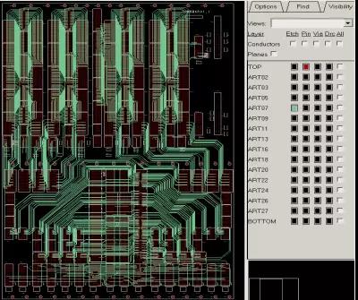
The stack of PCB is composed of power layer, ground layer and signal layer. The signal layer, as its name implies, is the wiring layer of signal lines. The power layer and the ground layer are sometimes collectively referred to as the plane layer.
In a small number of PCB designs, wiring on the power ground plane layer or power and ground networks on the wiring layer is used. For this mixed type of layer PCB design, it is collectively called the signal layer.
SMT basic process components include: screen printing (or dispensing), placement (curing), reflow soldering, cleaning, testing, and repair
1. Silk screen: Its function is to print solder paste or patch glue onto the PCB pads to prepare for the soldering of components. The equipment used is a screen printing machine (screen printing machine), located at the forefront of the SMT production line.
2. Dispensing: It is to drip glue onto the fixed position of the PCB board, and its main function is to fix the components on the PCB board. The equipment used is a glue dispenser, located at the forefront of the SMT production line or behind the testing equipment.
3. Mounting: Its function is to accurately mount the surface mount components to the fixed position of the PCB. The equipment used is a placement machine, located behind the screen printing machine in the SMT production line.
4. Curing: Its function is to melt the patch glue, so that the surface assembly components and the PCB board are firmly bonded together. The equipment used is a curing oven, located behind the placement machine in the SMT production line.
5. Reflow soldering: Its function is to melt the solder paste, so that the surface mount components and the PCB board are firmly bonded together. The equipment used is a reflow oven, located behind the placement machine in the SMT production line.
6. Cleaning: Its function is to remove the solder residues such as flux that are harmful to the human body on the assembled PCB board. The equipment used is a washing machine, and the location may not be fixed, it may be online or offline.
7. Inspection: Its function is to inspect the welding quality and assembly quality of the assembled PCB board. The equipment used includes magnifying glass, microscope, online tester (ICT), flying probe tester, automatic optical inspection (AOI), X-RAY inspection system, functional tester, etc. The location can be configured in a suitable place on the production line according to the needs of the inspection.
8. Rework: Its function is to rework the PCB boards that have failed to detect faults. The tools used are soldering irons, rework stations, etc. Configured at any position in the production line.