Causes of PCB board bending and warping and prevention methods
In the PCB manufacturing process, most of the circuit boards are prone to board bending and warping when passing through Reflow. If it is serious, it may even cause components such as empty soldering and tombstones. How can I overcome it?
To be honest, the cause of each plate bending and plate warping may be different, but it should all be attributed to the stress applied to the board that is greater than the stress that the board material can withstand. When the board is subjected to uneven stress Or when the ability of each place on the board to resist stress is uneven, the result of board bending and board warping will occur.
Where does the stress on the board come from? In fact, the biggest source of stress in the Reflow process is temperature. Temperature not only makes the circuit board soft, but also distorts the circuit board. Coupled with the material characteristics of thermal expansion and contraction, it is the main cause of board bending.
Then why do some boards have different degrees of bending and warping?

Before understanding the problem of board bending and board warpage, I suggest you refer to this article on the real cause analysis and prevention of PCB explosion. Some of the content will be related.
1. The uneven copper surface area on the circuit board will worsen the bending and warping of the board.
Generally, a large area of copper foil is designed on the circuit board for grounding purposes. Sometimes a large area of copper foil is also designed on the Vcc layer. When these large area copper foils cannot be evenly distributed on the same circuit board At this time, it will cause the problem of uneven heat absorption and heat dissipation. Of course, the circuit board will also expand and contract with heat. If the expansion and contraction cannot be performed at the same time, it will cause different stress and deformation. At this time, if the temperature of the board has reached Tg The upper limit of the value, the board will begin to soften, causing permanent deformation.
2. The connection points (vias) of each layer of the PCB will limit the expansion and contraction of the board
Today's circuit boards are mostly multi-layer boards, and there will be rivet-like connection points (via) between the layers. The connection points are divided into through holes, blind holes and buried holes. Where there are connection points, the board will be restricted. The effect of expansion and contraction will also indirectly cause plate bending and plate warping.
3. The weight of the circuit board itself will cause the board to dent and deform
Generally, the reflow furnace uses a chain to drive the circuit board forward in the reflow furnace, that is, the two sides of the board are used as fulcrums to support the entire board. If there are heavy parts on the board, or the size of the board is too large, It will show a depression in the middle due to the amount of seed, causing the plate to bend.
4. The depth of the V-Cut and the connecting strips will affect the deformation of the jigsaw
Basically, V-Cut is the culprit that destroys the structure of the board, because V-Cut cuts V-shaped grooves on the original large sheet, so the V-Cut is prone to deformation.
How can we prevent the board from bending and warping when the board passes through the reflow furnace?
1. Reduce the effect of temperature on the stress of the board
Since "temperature" is the main source of board stress, as long as the temperature of the reflow oven is lowered or the rate of heating and cooling of the board in the reflow oven is slowed, the occurrence of plate bending and warpage can be greatly reduced. However, other side effects may occur, such as solder short circuit.
2. Using high Tg sheet
Tg is the glass transition temperature, that is, the temperature at which the material changes from the glass state to the rubber state. The lower the Tg value of the material, the faster the board starts to soften after entering the reflow oven, and the time it takes to become soft rubber state It will also become longer, and the deformation of the board will of course be more serious. Using a higher Tg plate can increase its ability to withstand stress and deformation, but the price of the material is relatively high.
3. Increase the thickness of the circuit board
In order to achieve the purpose of lighter and thinner for many electronic products, the thickness of the board has left 1.0mm, 0.8mm, or even 0.6mm. Such a thickness must keep the board from deforming after the reflow furnace, which is really difficult. It is recommended that if there is no requirement for lightness and thinness, the thickness of the board should be 1.6mm, which can greatly reduce the risk of bending and deformation of the board.
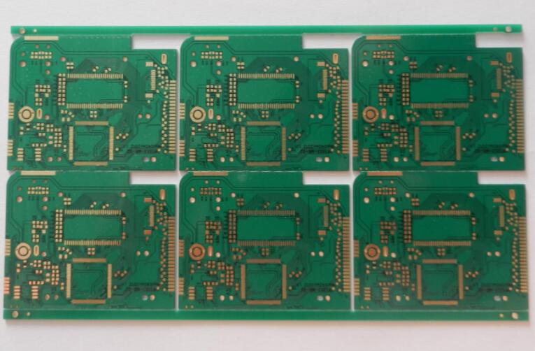
4. Reduce PCB size and reduce the number of puzzles
Since most of the reflow furnaces use chains to drive the circuit board forward, the larger the size of the circuit board will be due to its own weight, dent and deformation in the reflow furnace, so try to put the long side of the circuit board as the edge of the board. On the chain of the reflow furnace, the depression and deformation caused by the weight of the circuit board can be reduced. The reduction in the number of panels is also based on this reason. That is to say, when passing the furnace, try to use the narrow edge to pass the furnace direction as far as possible. The amount of depression deformation.
5. Used furnace tray fixture
If the above methods are difficult to achieve, the last is to use a reflow carrier/template to reduce the amount of deformation. The reason why the reflow carrier/template can reduce the bending of the plate is because it is hoped whether it is thermal expansion or cold contraction. The tray can hold the circuit board and wait until the temperature of the circuit board is lower than the Tg value and start to harden again, and can also maintain the size of the garden.
If the single-layer pallet cannot reduce the deformation of the circuit board, a cover must be added to clamp the circuit board with the upper and lower pallets. This can greatly reduce the problem of circuit board deformation through the reflow furnace. However, this furnace tray is quite expensive, and manual labor is required to place and recycle the trays.
6. Use Router instead of V-Cut's sub-board
Since V-Cut will destroy the structural strength of the panel between the circuit boards, try not to use the V-Cut sub-board or reduce the depth of the V-Cut.