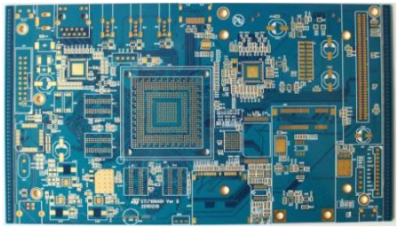
During heating and subsequent cooling cycles,the BGA package or PCB maybe warpage.This situation will cause the package to become a bow with the lower sides of the center raised. The bridging found in the X-ray examination means that the heating-cooling cycle pushes the corner up or down,or causes an open circuit. These problems can be found in the endoscopy or visual inspection. If the PCB is warped, it may cause an open circuit or a short circuit on other component areas.
Causes of these problems
The warpage of BGA and PCB is caused by the mismatch of the coefficient of thermal expansion (CTE) between the materials of various packaging components, such as substrates, silicon chips, and EMC packaging materials. When placing and moving, the rate of temperature increase will affect the uniform temperature distribution of the entire component, so the rate of temperature rise has an indirect relationship with the magnitude of warpage.

Moreover,when other conditions are the same,the larger the package,the greater the possibility of warping.Of course, the type of rework heating method (hot air rework system, infrared heating (IR), hot air reflow oven, vapor phase oven, etc.) will also affect the warpage. Use low-CTE thermally conductive materials, which can be customized CTE, to partially or completely eliminate this problem.
Some ball grid arrays (PBGAs) that use a plastic case include a heat spreader, which causes the top of the BGA package to expand at a faster rate than the bottom; this plastic expansion pulls the corners of the BGA downward. The moisture in the BGA may also cause warpage, because the components have to spread in the middle. In these cases, the corners of the BGA may curl upward.
Through a series of experimental designs, you can confirm which part (BGA or PCB) is warping. Experiments by isolating the pull and push surfaces can help determine how to solve this problem.
How to reduce warpage
When the BGA warps, the corners of the BGA will have the greatest displacement, which may cause a large number of open circuits and bridges. Similarly, the circuit board may bend up or down, pushing the solder paste inward, causing bridges or open circuits. These conditions should be found through visual inspection or X-ray inspection.
One way to minimize warpage is to slow down the heating and cooling process. The temperature ramps up during the preheating process, and the temperature drops during the cooling process. Of course, now you don't want to make the temperature drop too slow during cooling, this is because you don't want to create a coarse-grained structure. In the electronics manufacturing industry, appropriate trade-offs need to be made.
Controlling humidity sensitive devices (MSD), including circuit boards and components, is another way to reduce the effects of warpage. The J-STD-0033 and JEDEC guidelines for humidity handling are the best reference guidelines for the proper handling of MSD. If their warpage is related to moisture absorption, pre-baking the circuit boards and components, and then keeping them dry in a dry environment, can alleviate the warpage problem. Limiting exposure time and understanding the MSD levels of circuit boards and components will also play a major role in reducing warpage related to moisture absorption.
By using the solder paste produced according to the formula, the pillow effect can be reduced, and it can be used in conjunction with the appropriate solder paste, which can also limit the influence of solder ball warpage.
By appropriately designing the volume of solder paste applied to each pad position, some problems related to PCB and device warpage can be effectively limited. In some cases, the pads are transitioned during printing, and in other cases, the volume of solder paste on the pads is reduced during printing, which may compensate for the effects of warpage. For example, when the BGA is bent inward toward the PCB, an obvious short circuit may appear. In these areas, it may be necessary to reduce the volume of solder paste printed as much as possible. On the contrary, in the area where the warped BGA bends "off" the circuit board, printing a larger volume of solder paste may be the best solution.