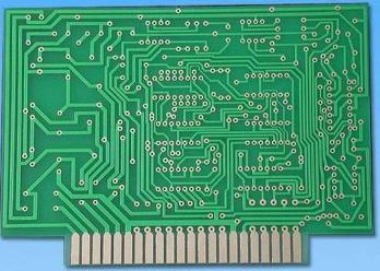
1. PCB size and appearance inspection
The content of PCB size inspection mainly includes the directness of processing holes, spacing and tolerances, PCB edge dimensions, etc. The content of appearance defect inspection mainly includes: the alignment of the solder mask and the pad; whether the solder mask has abnormal conditions such as impurities, peeling, wrinkles, etc.; whether the reference mark is qualified; whether the circuit conductor width (line width) and spacing are consistent Requirements; Whether the multilayer board is peeled off, etc. In practical applications, special equipment for PCB appearance testing is often used to detect it. Typical equipment is mainly composed of computers, automatic workbenches, and image processing systems. This system can detect the inner and outer layers of multi-layer boards, single/dual panels, and base map films; it can detect broken lines, overlapping lines, scratches, pinholes, line widths, rough edges, and large edges. Area defects, etc.

Unreasonable design and improper processing of the process may cause the warpage and distortion of the PCB. The test method is to expose the tested PCB to a representative thermal environment of the assembly process and conduct a thermal stress test on it. Typical thermal stress testing methods are spin dipping test and solder float test. In this test method, the PCB is immersed in molten solder for a certain period of time, and then taken out for warpage and distortion testing. The PCB circuit defect AOI detection device and detection principle are shown in the figure.
The manual method of measuring the PCB is: close the three corners of the PCB to the desktop, and then measure the distance from the fourth corner to the desktop. This method can only be used for rough estimation, and more effective methods include the application of ripple imaging technology. The method of corrugated image is: place a 100-inch grating on the PCB under test, and set a standard light source to shoot on the PCB through the grating at an incident angle of 45°C. The grating produces a grating image on the PCB, and then a CCD is used. The camera observes the raster image directly above the PCB. At this time, the geometric interference fringes generated between the two gratings can be seen on the entire PCB. This fringe shows the offset in the Z direction. The number of fringes can be counted to calculate the offset height of the PCB, and then converted by calculation Into the degree of warpage.
Patch processing
2. PCB solderability test
The solderability test of PCB focuses on the test of pads and plated through holes. Standards such as IPC-S-804 specify the solderability test method of PCB, which includes edge dipping test, rotating dipping test, wave dipping test and solder Bead test etc.
3. PCB solder mask integrity test
Generally, dry film solder mask and optical imaging solder mask are used on PCB, these two kinds of solder mask have high resolution and immobility. Dry film solder mask is laminated on the PCB under pressure and heat. It requires a clean PCB surface and an effective lamination process. The surface of the solder mask tin-lead alloy has poor adhesion, and under the impact of thermal stress generated by reflow soldering, the phenomenon of peeling and breaking from the PCB surface often occurs. This kind of solder mask is also brittle, and may cause micro-cracks under the influence of heat and mechanical force during leveling. In addition, physical and chemical damage may also occur under the action of cleaning agents. In order to find out these potential defects of dry film solder mask, strict thermal stress test should be carried out on PCB during incoming material inspection. When the solder mask peeling phenomenon is not observed during the test, the PCB sample can be immersed in water after the test, and the capillary action of the water between the solder mask and the PCB surface can be used to observe the solder mask peeling phenomenon. The PCB specimen can also be immersed in the SMA cleaning agent after the test to observe whether it has physical and chemical effects with the solvent.
4. PCB internal defect detection
The detection of internal defects of PCB generally adopts microsection technology, and the specific detection method is clearly stipulated in relevant standards such as IPC-TM-650. The main inspection items for microsection inspection include the thickness of the copper and tin-lead alloy coatings, the alignment of the internal conductors of the multilayer board, the laminated voids and the copper cracks.