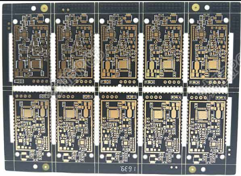
PCB parallel termination
PCB parallel termination is mainly to add pull and/or pull impedance as close as possible to the load end to achieve impedance matching of the terminal. According to different application environments, PCB parallel termination can be divided into the following types:
(I) Simple PCB parallel termination. This termination method is to simply add a resistor RT (RT=Z0) pulled to the GROUND at the load end to achieve matching. The condition for adopting this termination is that the drive end must be able to provide the drive current when the output is high to ensure that the high level voltage through the termination resistor meets the threshold voltage requirement. When the output is in a high-level state,

this PCB parallel termination circuit consumes too much current. For a 50Ω termination load, maintaining a high TTL level consumes up to 48mA. Therefore, it is difficult for general devices to reliably support this type of termination. Connect the circuit
(II) Thevenin PCB parallel termination is the voltage divider type termination. It uses a pull-up resistor R1 and a pull-down resistor R2 to form a termination resistor, and absorbs reflections through R1 and R2. The selection of the resistance values of R1 and R2 is determined by the following conditions. The maximum value of R1 is determined by the maximum rise time of the acceptable signal (which is a function of the RC charge and discharge time constant), and the small value of R1 is determined by the current sink value of the drive source. The choice of R2 should meet the logic high level requirement of the circuit when the transmission line is disconnected. Thevenin equivalent impedance can be expressed as:
Here, RT is required to be equal to the transmission line impedance Z0 in order to achieve the best match. Although this termination scheme reduces the requirements for the drive capability of the source-side devices, the resistance R1 and R2 connected between VCC and GROUND has been drawing current from the system power supply, so the DC power consumption is relatively large.
(III) Active PCB parallel termination
In this termination strategy, the termination resistor RT (RT=Z0) pulls the load terminal signal to an offset voltage VBIAS. The selection basis of VBIAS is to make the output drive source capable of drawing current for high and low level signals. This type of termination requires an independent voltage source with the ability to sink and sink current to meet the requirements of the jump speed of the output voltage. In this termination scheme, if the offset voltage VBIAS is a positive voltage and the input is at a logic low level, there will be DC power loss. If the offset voltage VBIAS is a secondary voltage, there will be a DC power loss when the input is at a logic high level.
(IV) PCB parallel AC termination
The PCB parallel AC termination uses a resistor and capacitor network (series RC) as the termination impedance. The termination resistance R must be less than or equal to the transmission line impedance Z0, and the capacitance C must be greater than 100pF. Multilayer ceramic capacitors of 0.1uF are recommended. The capacitor has the function of blocking low frequency and high frequency, so the resistance R is not the DC load of the driving source, so this termination method does not have any DC power consumption.