The biggest difference between PCB multi-layer boards and single-sided and double-sided boards is the addition of internal power and ground planes. The power supply and ground network are mainly routed on the power supply layer. There are conductive metals on both sides of each substrate layer on the PCB multi-layer board, and a special adhesive is used to connect the boards together, and there is an insulating material between each board. However, PCB multilayer wiring is mainly based on the top and bottom layers, supplemented by intermediate wiring layers.
Therefore, the design of the multilayer PCB board is basically the same as the design method of the double-sided board. The key is how to optimize the wiring of the internal electrical layer to make the wiring of the circuit board more reasonable. The inevitable product of multi-functional development, large capacity and small volume.
With the continuous development of electronic technology, especially the extensive and in-depth application of large-scale and very large-scale integrated circuits, multilayer PCBs are developing rapidly in the direction of high density, high precision and high-level digitization. Fine lines, small aperture penetration and blind hole technologies (such as buried vias and high plate thickness to aperture ratio) can meet market needs. PCB multilayer printed boards are widely used in the manufacture of electronic products due to their flexible design, stable and reliable electrical performance and excellent economic performance.

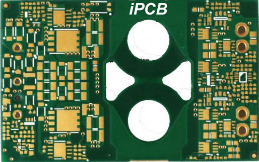
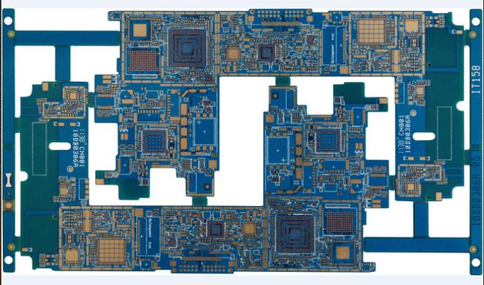
PCB multi-layer boards
Especially with the extensive and in-depth application of large-scale and very large-scale integrated circuits, multi-layer PCB are developing in the direction of high density, high precision and high level of digitization. Fine lines, small aperture penetration and blind hole technologies (such as buried vias and high plate thickness to aperture ratio) can meet market needs. PCB multilayer printed boards are widely used in the manufacture of electronic products due to their flexible design, stable and reliable electrical performance and excellent economic performance. Especially with the extensive and in-depth application of large-scale and very large-scale integrated circuits, multilayer PCBs are developing in the direction of high density, high precision and high-level digitization.
Fine lines, small aperture penetration and blind hole technologies (such as buried vias and high plate thickness to aperture ratio) can meet market needs. PCB multilayer printed boards are widely used in the manufacture of electronic products due to their flexible design, stable and reliable electrical performance and excellent economic performance. Blind technology such as blind hole technology and high plate thickness to aperture ratio can meet market demand.
PCB multilayer boards are widely used in the PCB manufacture of electronic products due to their flexible design, stable and reliable electrical performance and excellent economic performance. Blind hole technology, high plate thickness to aperture ratio and other blind technology can meet market demand. PCB multilayer printed boards are widely used in the manufacture of electronic products due to their flexible design, stable and reliable electrical performance and excellent economic performance.