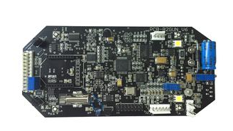
A comparison of the hole diameter of the 300um drilled pin hole in the general FR4 circuit board and the 100um pin hole in the PCB build-up circuit board. Since the signal lines are arranged along the X direction and the Y direction, a bolt hole must be arranged at the intersection of the X and Y direction wires to allow conduction between the upper and lower layers. The bolt holes are arranged in an oblique line direction, and this oblique line arrangement can achieve the maximum number of bolt holes. Generally, the density index of high-density PCB circuit boards is expressed by the density of pin holes. The number of bolt holes that can be accommodated per inch square area is expressed in units of VPSG. The pinhole density of the FR4 circuit board in Figure 6.1 is only 4VPSG, while the pinhole density of the PCB build-up circuit board is as high as 20VPSG. In addition to the build-up circuit board plane circuit density is 3 times that of the general FR4 printed circuit board, since the insulation layer thickness of the build-up circuit board is only 40um and thinner than the FR4 circuit board, the density in the Z direction is also twice that of the FR4 circuit board. Therefore, the circuit density of the entire build-up circuit board can exceed 10 times that of the general FR4 circuit board. Since the circuit density of the build-up circuit board is much higher than that of the FR4 printed circuit board, if the precision required for the manufacturing process cannot be ensured, the production yield of the build-up circuit board will be greatly reduced.
The glass fiber substrate of the traditional FR4 printed circuit board is formed by pressing the glass fiber cloth containing epoxy resin and the copper foil, and then forming the conductive perforation between the upper and lower layers by mechanical drilling, and then forming it by photo-etching. line. Therefore, part of the manufacturing process is mechanical processing, and part is chemical manufacturing.

PCB build-up circuit boards are basically completed by chemical processes except for a small part of the perforation process. Because the circuit density is much higher than the traditional FR4 circuit board inspection method for quality control. For the build-up circuit board, the control of the process error is very important, so how to choose the process control parameters and control process parameters is a very important work. However, because many process parameters cannot be directly inspected or observed directly, how to monitor these process parameters is one of the key points in determining whether the mass production technology of build-up circuit boards is mature or not.
Choosing the best printed circuit board process conditions
The biggest problem with build-up printed circuit boards stacked in sequence is that as the number of build-up layers increases, the yield of the process tends to decrease. The yield of the product can be obtained by multiplying the yield of each layer. Assuming that the process yield of each layer is 95%, the process yield is only 0.954=0.81 after overlapping four layers.
Therefore, the number of layers of the build-up printed circuit board should be as small as possible while meeting the functional requirements, and the function of the FR4 printed circuit board should be maximized in the design. The various applications introduced before can achieve the circuit functions required by the system through various combinations of the build-up circuit board and the base layer, and achieve the most appropriate combination in terms of size and cost. However, even FR4 printed circuit boards have more and more layers under the trend of high density since the 1970s. However, because of the high density of FR4 printed circuit boards, the number of layers that must be increased is very large and the cost has become very high., So there are not many examples actually used. In contrast, since the circuit density of each layer of the build-up circuit board can be very high, if the number of layers is increased, the density of the circuit board can be greatly increased.