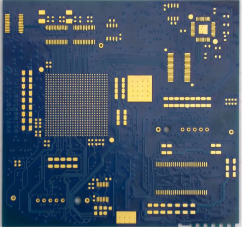
1. PCB wiring adjustment
I would like to ask a question: It takes time to adjust because of the unsatisfactory fabric of the machine. Generally, manual wiring is used. Most of the PCB boards that are used nowadays need to use a chip with a higher pin density to package the chip, and with a bus (ABUS, DBUS, CBUS, etc.), due to the high operating frequency, the lead should be as short as possible Naturally, dense signal lines are evenly distributed on a small area of the board.
I feel that it takes more time to adjust these dense signal lines. One is to adjust the distance between the lines to make them as even as possible. Because in the process of wiring, it is generally necessary to change the wiring from time to time. Every time you change it, you must re-even the spacing of each line that has been laid out. The more it goes to the end, the more this happens. The second is to adjust the width of the line so that it can accommodate the newly added line as much as possible in a certain width. Generally, there are many bends in a line, one bend is one section, manual adjustment can only be adjusted one by one, and it takes time to adjust.
If in the process of wiring, I can manually pull the wires roughly according to my idea, after the completion, the software can help me automatically adjust from these two aspects. Or even if the cloth is finished, if you want to change the thread, change it roughly, and then let the software adjust it. Even, in the end, I felt the need to adjust the package of the components, that is to say, the entire wiring needs to be adjusted and let the software do it. That would be much faster. I use Protel98. I know that this software can automatically adjust the distance of the component packaging but not the line spacing and line width. It may be that some of these functions are not yet available to me, or there are other ways. I would like to ask here.
Answer: Line width and line spacing are two important factors that affect the trace density. Generally, when designing a board with a higher operating frequency, it is necessary to determine the characteristic impedance of the trace before wiring. In the case of a fixed PCB stack, the characteristic impedance will determine the line width. The line spacing has an absolute relationship with the size of crosstalk (Crosstalk). The minimum acceptable line distance depends on whether the influence of crosstalk on signal time delay and signal integrity is acceptable. The minimum line distance can be obtained by pre-simulation by simulation software. In other words, before wiring, the required line width and minimum line distance should have been determined, and can not be changed at will, because it will affect the characteristic impedance and crosstalk. This is why most EDA wiring software does not change the line width and minimum line distance when doing automatic wiring or adjustment. If the line width and minimum line distance have been set in the wiring software, the convenience of wiring adjustment depends on the ability of the software winding engine. If you are interested in the company Expedition, try our winding engine,

2. About high-speed digital PCB
May I ask what is the principle of properly selecting the grounding point between the PCB and the case? In addition, the general PCB LAYOUT engineers always follow the DESIGN GUIDE/LAYOUT GUIDELINE. I want to know whether the general GUIDE is the hardware/system engineer or the senior PCB engineer? Who should Mainly responsible for the performance of the board-level system?
Answer: The principle of selecting the grounding point of the enclosure is to use the chassis ground to provide a low-impedance path for the returning current and control the path of this return current. For example, usually in the vicinity of high-frequency devices or clock generators, a fixed screw can be used to connect the ground layer of the PCB to the chassis ground to minimize the area of the entire current loop and reduce electromagnetic radiation. Who should be responsible for formulating the guidelines may have different arrangements for each company in different situations. The formulation of the guideline must have a full understanding of the operating principles of the entire system, chip, and circuit in order to formulate an achievable guideline that meets electrical specifications. So, from my personal point of view, hardware system engineers seem to be more suitable for this role. Of course, senior PCB engineers can provide experience in actual implementation, making this guideline better.
3. Circuit board DEBUG should proceed from those aspects.
Question: After the board is designed and produced, which aspects should DEBUG start with?
Answer: As far as digital circuits are concerned, first determine three things in order:
1. Confirm that all power supply values meet the design requirements. Some systems with multiple power supplies may require certain specifications for the order and speed of the power supplies.
2. Confirm that all clock signal frequencies are working properly and there are no non-monotonic problems on the signal edges.
3. Confirm whether the reset signal meets the specification requirements.
If these are normal, the chip should send out the first cycle (cycle) signal. Next, debug according to the operating principle of the system and the bus protocol.
4.How does the commonly used electronic PCB design software meet the requirements of circuit anti-interference?
Q: What kind of PCB design software is there now, how to use PROTEL99 to design a PCB that meets your requirements reasonably. For example, how to meet the requirements of high-frequency circuits, how to consider the circuit to meet the requirements of anti-interference?
Answer: I have no experience in using Protel, the following will only discuss the design principles.
High-frequency digital circuits mainly consider the influence of transmission line effects on signal quality and timing. Such as the continuity and matching of characteristic impedance, the selection of termination methods, the selection of topology methods, the length and spacing of traces, the control of clock (or strobe) signal skew, etc.
If the device has been fixed, the general anti-interference method is to increase the spacing or add ground guard traces
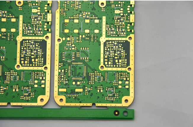
5. Question: When the size of the circuit board is fixed, if more functions need to be accommodated in the design, it is often necessary to increase the trace density of the PCB, but this may increase the mutual interference of the traces, and at the same time, the traces are too thin. So that the impedance cannot be lowered, introduce the skills in high-speed (>100MHz) high-density PCB design?
Answer: When designing high-speed and high-density PCBs, crosstalk interference (crosstalk interference) really needs special attention, because it has a great impact on timing and signal integrity. Here are a few points to note:
1. Control the continuity and matching of the characteristic impedance of the wiring.
2. The size of the trace spacing. The commonly seen spacing is twice the line width. It is possible to know the influence of trace spacing on timing and signal integrity through simulation, and find the minimum tolerable spacing. The result of different chip signals may be different.
3. Choose the appropriate termination method.
4. Avoid two adjacent layers with the same routing direction, even if there are traces overlapping up and down, because this kind of crosstalk is greater than the case of adjacent traces on the same layer.
5. Use blind/buried vias to increase the trace area. However, the manufacturing cost of the PCB board will increase.
It is really difficult to achieve complete parallelism and equal length in actual implementation, but it is still necessary to do it as much as possible. In addition, differential termination and common mode termination can be reserved to alleviate the impact on timing and signal integrity.