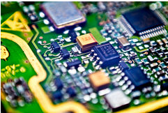
1. Overview PCB (printed circuit board), the Chinese name is printed circuit board, printed circuit board for short, is one of the important parts of the PCB industry. Almost every kind of electronic equipment, small electronic watches, calculators, large computers, communication electronic equipment, military weapon systems, as long as there are electronic components such as integrated circuits, are used for electrical interconnection between them, using printed circuit boards. In the larger electronic product research process, the most basic success factor is the design, recording, and manufacturing of the product's printed circuit board.
The design and manufacturing quality of printed boards directly affects the quality and cost of the entire product, and even leads to the success or failure of commercial competition. A printed circuit provides the following functions in an electronic device:
Provide integrated circuit and other electronic components fixing, assembly mechanical support.

Realize wiring and electrical connection or electrical insulation between various electronic components such as integrated circuits.
Provide the required electrical characteristics, such as characteristic impedance.
It is used for automatic welding, provides resistance for welding graphics, and provides recognition characters and graphics for component insertion, inspection and maintenance.
2. Some basic terms of printed board are as follows:
On an insulating substrate, according to a predetermined design, it is made of printed lines, printed elements or a combination of two conductive patterns, which is called a printed circuit. On an insulating substrate, conductive patterns that provide electrical connections between components and devices are called printed lines.
It does not include printing components.
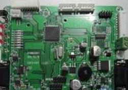
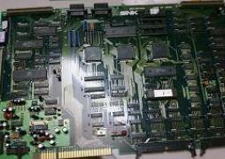
The printed circuit or printed line of the PCB finished board is called a printed circuit board or printed circuit board, also called a printed circuit board. According to whether the substrate used is rigid or flexible, printed boards can be divided into two categories: rigid printed boards and flexible printed boards. This year, the combination of printed boards is very flexible.
According to the number of layers of conductor patterns, it can be divided into single-sided, double-sided and multilayer printed boards.
The entire outer surface of the conductor pattern is printed on the same plane as the surface of the substrate, which is called a flat printed board.
For the terms and definitions of printed circuit boards, please refer to the national standard gb/t2036-94 "Printed Circuit Terminology".
After the electronic equipment uses the printed circuit board, due to the consistency of the similar printed circuit board, the error of manual wiring is avoided, and the automatic insertion or placement of electronic components, automatic welding, and automatic detection can be realized to ensure the quality of electronic equipment and improve labor. Productivity, cost reduction and easy maintenance. Printed circuit boards from single layer to double-sided, multi-layer and flexible, and still maintain their own development trend
Due to the continuous development of high precision, high density and high reliability, continuous reduction of volume, cost reduction, and performance improvement, the printed circuit board will still maintain a strong vitality in future electronic equipment development projects.
Third, the sign of the technical level of the printed circuit board:
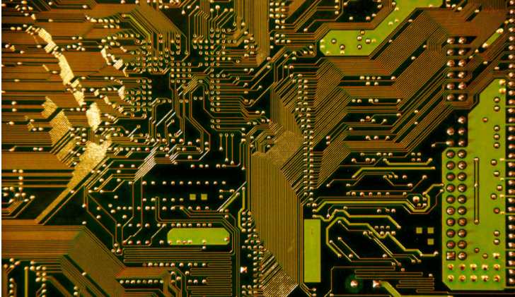
Double-sided and multi-layer porous metalized printed circuit board PCB technology level marking: mass production of double-sided metalized printed circuit board, 2.50 or 2.54mm standard grid intersection between two pads, can be used as the root number of the wire symbols of. Place a wire between the two pads. This is a low-density printed circuit board with a wire width greater than 0.3mm. Two wires are placed between two pads, which are medium-density printed circuit boards, and the wire width is about 0.2mm. Place three wires between the two pads. These two pads are high-density printed boards with a line width of about 0.1-0.15mm.
Placing four wires between the two pads can be counted as an ultra-high density printed circuit board with a line width of 0.05-0.08mm.
Foreign magazines have introduced printed circuit boards that can place five wires between two pads.
For multi-layer boards, the aperture size and the number of layers should also be used as a comprehensive measurement mark.
4. The development trend of PCB advanced manufacturing technology.
This article summarizes the development trend of PCB manufacturing technology at home and abroad in the future, namely, the development direction of high density, high precision, fine aperture, fine line, fine pitch, high reliability, multi-layer, high-speed transmission, light and thin, in production At the same time increase productivity, reduce costs, reduce pollution.