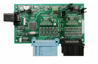
For each of these PCB categories, the plating and non-plating categories should be identified.
1. Welded
Plated through holes (PLTH) (including through holes)
Non-plated through hole (NPTH)
2. Not to be welded
Through hole being welded
3. Non-plated through holes with PCB pads and PCB without pads (NPTH)
The designer must first know whether the PCB pad is confirmed to be soldered or not. This information helps the engineer decide whether the pad calculation is for soldering or for the smallest hole ring. If the pad is not soldered, the standard ring hole can be used and the assembly requirements remain unchanged.
A through hole is just a plated through hole without soldering. In each assembly or application, it does not require calculation to confirm the pad size, but requires a simpler calculation for the smallest ring hole or the smallest and most economical size that can carry enough current.
4. Non-welded through holes
The minimum orifice ring consists of two different items. When the manufacturer talks about the minimum orifice ring, it refers to the minimum orifice ring required by the standard or the designer's mark plus its own orifice ring requirements. The orifice ring specified by IPC or other standards is the smallest orifice ring required to complete the printed board.
For a 0.008 inch hole, the smallest land diameter should be a 0.031 inch. Again, it must be noted that this is a minimum value. Don't use it unless necessary. The recommended size is at least 0.002 inches larger than the minimum diameter. The values in these examples are based on conventional processes.
For the outer land ring, it should be at least 0.002 inches thicker than the plating layer (circular), and for the inner land ring, it should be at least 0.001 inches thicker than the plating. The effective plating thickness is 0.0025-0.0030 inches.
5. Through holes being welded

Except that the outer surface area must be larger to enhance heat dissipation to avoid poor soldering problems, most of the rules apply to the through holes being soldered. If possible, for consistency and ease of calculation, unless simplified pads are required, the inner pads should be the same as the outer pads. The reason is that the outer pad is soldered but the inner pad is not. The through hole to be soldered must increase in proportion to the pin diameter, because larger pins require more heat; and in order to connect the pins and the pads Evenly dissipate heat between the spaces, and the pads must be enlarged.
For soldering through-hole pads, there is a range of acceptable sizes. This range is not less than the smallest hole ring to twice the hole size. The diameter of the soldered pad is twice the diameter of the final hole.
These values are based on standard component lead materials and may vary with the type of material.
6. Thermal pad
Thermal connection is only a feature used/required for solder pads. Usually used in the plane layer or solid copper foil area, they are connected to three or four printed circuit boards on the pad in the shape of + or *. The actual PCB circuits are often called spokes because they look like bicycle spokes. The role of these radial parts on the pad is not only to connect the flat or three-dimensional copper foil area to the hole wall, but to reduce the heat dissipation effect of the copper foil area. The parallel ratio between the copper foil of the printed board and the component lead metal requires that the soldered through hole has a limited copper foil area, but it must maintain a sufficient area to make it have current-carrying capacity. Therefore, the combined width of the spokes is equal to the diameter of the pad. The thermal pad has the same diameter as the other inner pads. The area including the pads and spokes is called the thermal outer diameter. This distance is equal to the inner diameter * 1.5.
7. Non-plated through holes
There are two types of non-plated through holes: with pads and without pads. It is important to note that the pads are electroplated or not electrified. During the electroplating process, if the pad is present, the hole must be electroplated with copper foil. If the pad is not electroplated, it must be drilled after the electroplating process, resulting in additional costs. NPTH without pads may be drilled as many times as other components.
8. Non-plated through holes with pads
Non-plated through holes refer to electroless plating in the holes that pass through the pads. This means that in addition to the normal copper adhesive, there is no additional carrier to support the pad. For this reason, the pad must be large enough to facilitate bonding and support the pad during heating or soldering. IPC defines the perforated ring of this non-supported pad as 0.006 inches. If the pad is to be soldered, this data should be larger.
9. Non-plated through holes, no pads
General NPTH is as large as a hole without pads or plated on the hole wall on a PCB printed board. Such as mounting holes, access holes for screw adjustment, and transfer holes for wires. Non-plating or ring ring requirements are necessary. General PCB through holes are different from other PCB holes because they are not electroplated or soldered.