If the transmission line system of the multilayer board is to reach 60±10%Ω, it is easy, but it will be a little difficult to reach 75±5%Ω, or even 50±5%Ω. The error of 5% is even for those with higher technical specifications. It is also not common in application, but some customers still have a requirement of ±5% for impedance control accuracy.
The TOP layer has single-line impedance requirements, and the reference layer is the second layer. The single-line impedance line width W1 requires 12.0MIL, and the impedance requires 50±5%Ω (50±2.5Ω). Its structure is as follows:
How can customers meet such strict impedance control accuracy requirements? Let's talk about how we control it.
Simulation calculation of PCB characteristic impedance
For boards with impedance control requirements, at present, a common practice in PCB factories is to design some impedance samples at appropriate positions on the side of the PCB production imposition board. These impedance samples have the same layering and impedance line structure as the PCB. Before designing the impedance sample, some impedance calculation software will be used to simulate the impedance in advance in order to predict the impedance. It is used by many PCB manufacturers and has simple operation and powerful functional computing capabilities.
But no matter how powerful the system is, its computing power and field solution tools for calculating impedance all rely on the use of "ideal" materials, and there will always be a certain deviation between the results of simulation calculations and the actual measured impedance results. Therefore, when the customer's impedance control accuracy is required to be ±5%, it is particularly important to use software with higher calculation accuracy to perform more accurate simulation predictions.

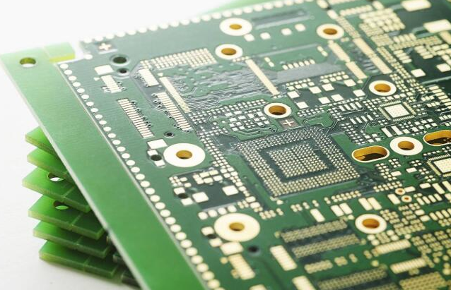
PCB production process control
Use parallel light exposure machine for production
Because non-parallel light is a point light source, the emitted light is scattered light. Therefore, the light passes through the film and enters the photosensitive dry film or other liquid resist film. It is exposed at various angles and is exposed and developed. There will be a certain deviation between the pattern and the pattern on the negative. The parallel light is irradiated to the photosensitive dry film or other liquid resist film in the vertical direction for exposure. Therefore, the width of the exposed wire on the photosensitive layer will be very close. The width of the wire on the film negative, in this way, can get a more accurate wire width, thereby reducing the impact of this deviation on impedance.
Thin copper foil is selected for outer base copper
Due to the rapid development of fine circuits, thin copper foils have been extensively developed and are fully used. The thickness of copper foil has been mainly from 1OZ to 1/2OZ in the early years, and 1/3OZ and 1/4OZ have also been developed early. Even thinner ones such as 1/7OZ copper foil. Because the thinner copper foil thickness is conducive to manufacturing and controlling the width of the wire and the integrity of the wire, thereby helping to ensure the accuracy of impedance control. Since the customer's outer layer copper thickness is 1OZ, we chose 1/3OZ copper foil for the outer layer of the four-layer board. After the subsequent electroplating, it can reach the customer's surface copper thickness of 1OZ copper. Thickness requirements, which not only meets the customer's requirements for the copper thickness on the surface, but also facilitates the control of the uniformity of the wire width during etching.
Laminating with copper foil energized heating press
There are two heating methods for the laminator, electric heating and steam heating, and what we use is a multilayer vacuum press produced by the Italian CEDAL company with ADARA technology. The system uses a coil of copper foil to surround the prepreg and inner layer board. The copper foil is energized in the laminator to achieve the heating effect and temperature distribution. The temperature distribution of the entire laminate can reach 177±2°C. Due to the fast heating, the temperature distribution is uniform and the pressure During the bonding process, the resin fluidity is relatively uniform, the thickness and flatness of the laminated board can reach ±0.025mm, and the thickness of the interlayer dielectric layer is relatively uniform.
Use whole plate electroplating for production
In order to obtain a relatively uniform thickness and width of the wire to ensure that the impedance is within the specified tolerance range, the PCB is directly produced by full-board electroplating after the holeization, in which the current density is appropriately reduced. Since the PCB directly enters the full-board electroplating after holeization, under certain plating solution conditions, the entire board's board surface receives a uniform current density, so the copper thickness of the entire board surface and the hole is relatively uniform This is beneficial to control the uniformity of surface copper thickness and wire width (because uneven copper thickness will bring disadvantages to etching uniformity), which is beneficial to control the characteristic impedance of the PCB and reduce its volatility.
PCB impedance measurement
PCB impedance measurement is usually done using a time domain reflectometer (TDR), and TDR (time domain reflectometer) has become an established technique for measuring the characteristic impedance of a printed circuit board. The impedance measurement is also very important for the characteristic impedance with an accuracy of ±5%. It is necessary to ensure the accuracy of the measurement, otherwise it will cause the board with qualified impedance to be falsely detected as unqualified.