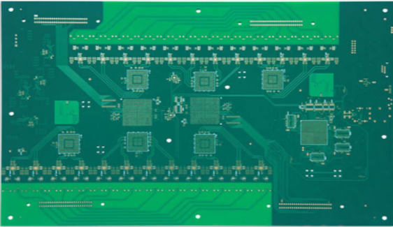
One, the method of PCB yin and yang board proofing
What does PCB paneling mean? The so-called PCB paneling means that when the project is finished drawing the PCB design, the drawn single PCS is pieced together into a large work board. V-Cut and process are reserved according to the shape of the product and the application field. The process of placing fixing holes and optical positioning points is called "PCB puzzle". So how to put together PCB Yin-Yang board proofing? What is the difference between PCB Yin-Yang board and conventional PCB assembly board? Here is a brief introduction to the correct method of PCB Yin-Yang board: 1. Copy the drawn PCB diagram to The newly-created PCB file is not in the middle, make a special paste, and select the PCB file to flip it, and then rotate the PCB file 180° counterclockwise.2. After copying the PCB file, perform "Special Paste" again, and choose the middle two items and do not re-copper
3. After copying the PCB file, select the move command to support it, an option will appear at this time, select "YES", the selected PCB file can be moved with the mouse at this time, press the "M" key, and it will appear In the dialog box, select "Flip Selection", turn the PCB file over, adjust the position to your desired position, select all the files again and execute the "move command" as before, drag the file and press the "Y" key to rotate 180° and place it in Specify the location. 4. After drawing the PCB file into the number of panels you need, before the formal production, the PCB process edge (3mm or 5mm) will be set according to the customer's requirements, and the "keep-out" layer will be selected for drawing.

Add "positioning hole" and "Mark point" on top, and finally use any layer such as "Overlay" layer or "keep-out" layer to mark V slot
Summary: There are differences in the number of PCB panels of different shapes. The salesman should communicate with the customer for the problem of the panel during the quotation process, such as: the number of PCB panels, the direction of the PCB panels, whether it is necessary to add process edges, and the craftsmanship. How many mm to add, whether to add Mark points according to the normal position, whether to add a moment between the single PCS, how many mm to add a moment, and other related issues, so that the engineering department can follow-up processing the data, and there is no need to repeatedly and continuously confirm with the customer NS.
Second, the common detection methods of PCB circuit boards
Manufacturing PCB circuit boards is a very complicated process. How to manage and control the quality of circuit boards is a problem that manufacturers have been focusing on. Here is a summary of the four common testing methods for PCB circuit boards. :1. Appearance size inspection: size inspection includes: the directness of processing holes, spacing and tolerances, PCB edge dimensions, etc. Appearance inspection includes: solder mask/pad alignment, presence of impurities, peeling, wrinkles and other abnormal phenomena in the solder mask, whether the reference mark is qualified, whether the circuit conductor width (line width)/spacing meets the requirements, multi-layer Whether the board is peeled off or not. When the design is not contracted or the process is not handled properly, warpage and distortion may occur. In this case, the correct test method is to expose the PCB to be tested to a representative thermal environment of the assembly process. Then the thermal stress test is performed on it. After the PCB board is immersed in the melt for a period of time, it is taken out for warpage and distortion testing. The second is manual measurement, using special measuring instruments to check whether the PCB dimensional tolerances are controlled within the range of customer requirements.
2. Solderability test: refers to the test of pads and electroplated through holes. Standards such as IPC-S-804 specify the solderability test method of PCB, which includes edge dipping test, rotating dipping test, wave dipping test and solder Bead test etc. 3. Solder mask integrity test: It is divided into dry film solder mask and optical imaging solder mask. Both of these two kinds of solder mask have high resolution and immobility. The difference is that dry film solder mask is Laminated on the PCB circuit board under the action of pressure and heat, the PCB must be cleaned up in advance and the effective lamination process must be cleaned in advance. Due to the poor viscosity of the solder mask tin-lead alloy surface, it is caused by flow soldering. Due to the thermal stress impact, PCB surface peeling or cracking is extremely likely. It is precisely because of the brittle solder mask that microcracks can easily appear due to the influence of heat and mechanical force during leveling. It is prone to physical and chemical damage. In order to improve the PCB yield rate, it is necessary to find out these potential defects in the extreme, and the PCB board should be subjected to a thermal stress test when the PCB substrate is received.4. Internal defect detection: When detecting the internal defects of the multilayer board, microsection technology should be used to detect the thickness of the tin-lead alloy coating on the PCB board, the alignment of the conductor layers, and the laminated voids and copper cracks.