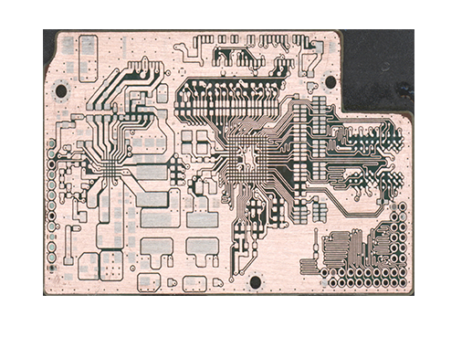
1. HDI high frequency blind hole circuit board production process
The two drilling processes used in the production of HDI high-frequency blind hole circuit boards are divided into two types: laser drilling and mechanical drilling blind/buried holes, then what is the difference between these two drilling processes, and the choice of drilling process in advance What is it! 1: Laser drilling: blind hole diameter is very small <=6MIL, special blind buried holes, such as blind holes from L1 to L2, and buried holes from L2 to L3, laser drilling is required. The principle of laser drilling is to vaporize or dissolve the plate into holes by absorbing the laser heat. Therefore, the plate must have light absorption. Therefore, the general RCC material is because there is no glass fiber cloth in the RCC and will not reflect light. Features of laser drilling production process: A). When the total number of layers of the circuit is N, the L2-Ln-1 layers are first produced according to the normal board process, B). After pressing the board, the process is changed to: --- >Drill LDI positioning holes--->Dry film--->Etch blind holes--->Laser drilling--->Drill through holes--->Sink copper----(normal process).
2: Mechanical drilling blind/buried holes: When the size of the drill bit>=0.20mm, mechanical drilling can be considered. What aspects should be paid attention to when mechanical drilling 1) Aspect ratio L/D: L=medium thickness+copper thickness, D= Blind hole/buried hole diameter. 2) Blind hole/buried hole electroplating film: *The diameter of the exposure point D=D-6 (MIL). *The exposure point film plus the alignment point, and its coordinates are consistent with the peripheral reference hole.

3) Blind holes that need to be filmed generally use pulse current (AC) during electroplating. When there are blind holes in the outer layer, a. Because the outer layer will flow out when the plate is pressed, a glue removal process is required after the plate is pressed; b. Because of the outer layer The surface of the board will be cleaned before drying. There is a grinding process. The electroless copper is very thin, only 0.05MIL to 0.1MI, so it is easy to wear off during grinding, so we will add a plate electroplating process to thicken the copper. Its related Processes such as: pressing plate-removing glue-drilling-sinking copper-plate electroplating-dry film-pattern electroplating.
Second, the basic difference between PCB blind buried vias and vias
What is a PCB blind hole board: blind hole, also known as "blind pass", refers to the connection between the outermost circuit in the printed circuit board and the adjacent inner layer with electroplated holes, because the opposite side cannot be seen from the surface of the PCB, Is called "blind hole board". In order to increase the space utilization rate between the circuit layers of the board, the blind hole board is just when it comes in handy. It can also be simply understood as a blind hole on the surface of the printed circuit board. Via hole. Buried vias refer to the links of any circuit inside the PCB, but they are not connected to the outside and cannot be observed with the naked eye on the surface of the PCB. Blind holes are located under the circuit board and have a certain depth. They are used to link the surface circuit with the lower circuit. The depth of the holes has a specified ratio. When making a buried blind hole board, you need to pay attention to the drilling depth must be just right. Electroplating is difficult in the hole, and the shallow hole cannot meet the process requirements.
What is a via hole: In addition to the usual drilled board, printed circuit boards also include blind holes, blind buried vias, vias, etc. The copper foil lines between conductive patterns in different layers use this hole to conduct or The disadvantage is that the copper-plated holes of the component pins or other reinforcing materials cannot be inserted. The PCB circuit board is formed by stacking multiple layers of copper foil, and the copper foil layers cannot communicate with each other because the copper foils of each layer They are covered with an insulating layer, so the signal link must be carried out with the help of via holes, which are called "via holes". It should be noted that not all PCB boards need to be made of via holes. The surface treatment process and process accuracy of PCBs in different fields are different. The via holes of the printed circuit board need to be plugged to meet customer requirements. In the traditional When printing circuit boards, aluminum plug holes are usually used, PCB board surface solder mask and plug holes are made of white mesh, making it more stable, reliable, and more complete. Vias help circuits connect and conduct each other. With the rise of the electronics industry, higher printing requirements have been put forward for printed circuit board technology. What conditions need to be met for the process of printing via hole plugging: a: There must be copper in the hole, and the solder mask can be plugged or not; b: There must be tin and lead in the hole, and a certain thickness is required to avoid the inflow of solder mask ink Hole, resulting in tin beads hidden in the hole, the through hole must have a solder mask plug hole, opaque, no tin rings and tin beads, and must be kept flat. PCB drilling is an important step in the process of manufacturing circuit boards. Generally speaking, drilling is to drill the required number of vias on the copper clad board according to the Gerber data provided by the customer. It has the function of providing electrical connection/fixing devices., Improper operation of this process can easily lead to problems such as under-drilled vias, over-drilled holes, and offset drilling, which may affect the performance and use of the circuit board, and at the same time, the subsequent process has not started, and it has already been scrapped and needs to be reopened. Material drilling, raw material waste not to mention also delays the production cycle.